Sponsored Post
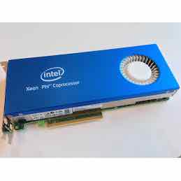 A coprocessor card needs to be designed to physically fit into an existing server, yet must contain a very high number of cores. Whereas on a main CPU design, the cores may take up significant real estate, designers must cram in over 50 cores on a smaller motherboard. In addition, the motherboard must be able to hold GDDR5 memory, memory controllers and miscellaneous electronics in order to communicate with the system CPU, but also perform floating point calculations in parallel.
The major functionality of the Intel Xeon Phi coprocessor is a chip that does the heavy computation. The current version utilizes up to 16 channels of GDDR5 memory. An interesting notes is that up to 32 memory devices can be used, by using both sides of the motherboard to hold the memory. This doubles the effective memory availability as compared to more conventional designs.
To communicate with the host, the Intel Xeon Phi coprocessor resides on the PCI Express bus, and is designed for the Gen 2 x16 standard. The Intel Xeon Phi coprocessor supports 64, 128, and 256 bye packet transmission. The card also contains Flash memory that contains the coprocessors startup code, which can be thought of as similar to the BIOS for an Intel Xeon CPU on a traditional motherboard.
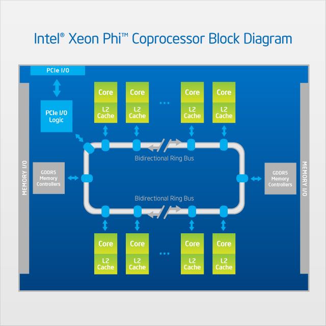
A block diagram of the Intel Xeon Phi coprocessor
In order for the high number of cores that are present on the Intel Xeon Phi coprocessor, a high speed ring based bidirectional on-die interconnect (ODI) is used. The communication over the ODI is transparent to the application that is running and is managed completely by the hardware. Each core has 512 KB of Level 2 cache, which stores data that might be reused. The ODI gives a core the ability to access the L2 cache or a different core with very high performance.
For developers, they can think of the Intel Xeon Phi coprocessor as Symmetric Multiprocessor (SMP) with shared uniform access memory, with each core having access to all of the memory at the same priority.
Source: Intel, USA
Transform Data into Opportunity Accelerate analysis: Intel® Data Analytics Acceleration Library.