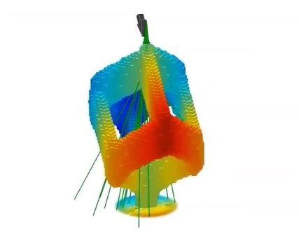
 In this video, ORNL researchers use supercomputers to simulate nanomanufacturing, the process of building microscopic devices atom by atom. Simulated here is the construction of a 250-nanometer 3-D cube by focused electron beam induced deposition. The electron beam (green cone) emits electrons (green lines) that interact with the precursor from the gas flux (grey arrow) to form solid deposits, simulated as pixels, on the substrate.
The process uses a 3-D simulation to guide the electron beam and replicate complex lattices and meshes between 10 nanometers and one micron in size. The model tracks electron scattering paths and the release of secondary electrons to predict the pattern of deposition on the surface of the material and visualize the final structure of an experiment.
Harald Plank, study co-author in Graz, Austria, said the ability to accurately design custom nanostructures “opens up a host of novel applications in 3-D plasmonics, free-standing nano-sensors and nano-mechanical elements on the lower nanoscale which are almost impossible to fabricate by other techniques.”
Read the Full Story.