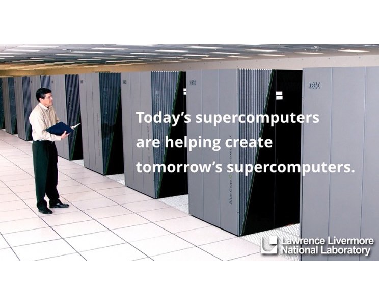
 Tomorrow’s top supercomputers will require chips built using advanced lithography far beyond today’s capabilities. Towards this end, Lawrence Livermore National Lab today announced a collaboration with ASML, a leading builder of chip-making machinery, to advance extreme ultraviolet (EUV) light sources toward the manufacturing of next-generation semiconductors.
Under a cooperative research and development agreement (CRADA), ASML is leveraging LLNL’s expertise in lasers and plasma physics and the ability to perform complex, large-scale modeling and simulation using high-performance computing. These combined resources will enable efficient and economical testing of new approaches targeted at further optimizing conversion efficiency, increasing source power and minimizing tin debris.
“Merging expertise, we demonstrated that computer codes developed by LLNL can accurately simulate ASML’s experimental data from its EUV light source,” said Steve Langer, computational physicist and project lead for LLNL. “Now that the simulation results and experimental data are aligned, we better understand the physics of EUV generation and can start to gain insight into what makes the light source perform well or poorly.”
ASML’s San Diego R&D and manufacturing facility specializes in the production of light sources used within microlithography scanners. ASML’s complex systems image a pattern on a silicon wafer, building up billions of transistors and circuit elements layer by layer, to make integrated circuits, or microchips, for the semiconductor industry. Its next-generation EUV technology will enable chipmakers to increase the number of transistors and significantly improve the performance of supercomputers and electronics.
EUV light is generated when a high-intensity carbon dioxide laser pulse hits droplets of tin, heating them to become plasma (ionized gas). The plasma emits EUV radiation that is then collected and transferred to a microlithography scanner, where it is used to expose silicon wafers. To increase EUV power, ASML researchers turned to high-fidelity computer simulations to better understand the physics of laser-produced plasmas and fill in the gaps for challenging lab experiments.
We anticipate our research partnership with LLNL will help us quickly zoom into the most promising technology development approaches, and thus shorten the time to market for future high-power EUV sources,” said Michael Purvis, senior scientist at ASML. “We’ve already extended our knowledge of tin plasmas through our joint modeling efforts that promise to help advance EUV power for high-volume manufacturing environments.”
In order to successfully build an accurate and predictive simulation, ASML engaged with LLNL’s High Performance Computing Innovation Center (HPCIC) and the National Ignition Facility (NIF) and Photon Science Directorate’s Advanced Photon Technologies (APT) Program to gain access to world-class supercomputers, software and deep domain knowledge, as well as experience in the application of advanced computing technologies. Livermore HPC capabilities and familiarity with high-energy-density physics occurring in laser-driven fusion experiments at NIF proved directly applicable to ASML’s technical challenges encountered in its advanced EUV lithography development.
This is a wonderful example of how expertise and capabilities across LLNL can be successfully brought together with leading industry experts to intensely focus on advancing photon sources of great importance to the commercial sector and broader society,” said Craig Siders, commercial technology development leader in NIF and Photon Science’s Advanced Photon Technologies Program.
Computer scientists at the National Energy Research Scientific Computing Center (link is external)at Lawrence Berkeley National Laboratory will leverage their expertise in laser plasma modeling software development to support the LLNL-ASML CRADA.
Our collaboration with ASML is just one example of how leading-edge companies can partner with Lawrence Livermore’s world-class HPC resources to advance technologies that stand to broadly benefit the computing industry as a whole, as well as help sustain U.S. leadership in science and technology,” added Fred Streitz, director of the HPCIC.
ASML is one of the world’s leading manufacturers of chip-making equipment. ASML’s guiding principle is continuing Moore’s Law toward ever smaller, cheaper, more powerful and energy-efficient semiconductors.