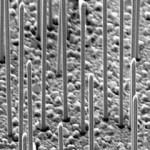
Search Results for: “lasers”

Proposed Legislation is How Not to Do Science

Search Results for: lasers

Over at the ISC Blog, Michael Feldman from Intersect360 Research writes that the proposed High Quality Research Act under consideration in Congress would severely restrict the types of research that could be funded.

Think of digital computers, the Internet, lasers, and genome sequencing, all of which are underpinned by basic science, and all of which received federal funding in their early stages. The silliest part of the proposed legislation is that it mandates that the research be “ground breaking,” an attribute that is impossible to predict. It’s like saying unless the research will win a Noble Prize, it’s not worth doing. Such wording reflects a fundamental misunderstanding of how science works.

Read the Full Story or check out the Full Committee Hearing – A Review of the President’s FY 2014 Budget Request for Science Agencies.

Read the entire post …

Posted in Computing Research, HPC, National and Legislative Action | Leave a comment

Record Simulations Conducted on Lawrence Livermore Supercomputer

Search Results for: lasers

Over at Lawrence Livermore, Breanna Bishop writes that researchers at LLNL have performed record simulations using all 1,572,864 cores of the Sequoia supercomputer. As the first supercomputer to exceed one million computational cores, Sequoia is also is No. 2 on the TOP500 with 16.3 petaflops of performance.

SIRIS simulation on Sequoia of the interaction of a fast-ignition-scale laser with a dense DT plasma.

The simulations were performed by Frederico Fiuza, a physicist and Lawrence Fellow at LLNL. Designed to study the interaction of ultra-powerful lasers with dense plasmas in a proposed method to produce fusion energy, the project is part of the U.S. Department of Energy’s Office of Fusion Energy Science Program.

Using the OSIRIS code, Fiuza demonstrated excellent scaling in parallel performance to the full 1.6 million cores of Sequoia. By increasing the number of cores for a relatively small problem of fixed size, what computer scientists call “strong scaling,” OSIRIS obtained 75 percent efficiency on the full machine. But when the total problem size was increased, what is called “weak scaling,” a 97 percent efficiency was achieved.

This means that a simulation that would take an entire year to perform on a medium-size cluster of 4,000 cores can be performed in a single day. Alternatively, problems 400 times greater in size can be simulated in the same amount of time,” Fiuza said. “The combination of this unique supercomputer and this highly efficient and scalable code is allowing for transformative research.”

Read the Full Story.

Read the entire post …

Posted in Compute, Computing Research, HPC, HPC Hardware | Leave a comment

Podcast: Radio Free HPC on the Energy Wall of Exascale

Search Results for: lasers

Power is a major challenge standing in the way of the Exascale computing. While the target is to consume 20 MW or less for an exascale machine, current technology trends will not take us there by 2018. In this podcast, the Radio Free HPC team discusses why this is such a tough challenge, where such a system might need to be hosted, and types of infrastructure that will need to be considered. Along the way, you’ll hear scary “power” music and figure out how this all relates to Mad Max, lasers, unicorns, and Planet of the Apes.

Download the MP3Download the VideoSubscribe on iTunesRSS Feed

Read the entire post …

Posted in Exascale, HPC, Podcast, Radio Free HPC | Leave a comment

IBM chips the laser light fantastic

Search Results for: lasers

By Timothy Prickett MorganGet more from this author

Boffins at IBM have come up with a better way to embed laser communications onto processor and memory chips using plain vanilla CMOS manufacturing processes, paving the way for three-dimensional chips integrating hundreds of processors, their main memory, and on-chip optical networks that will, it is hoped, allow for the creation of power-efficient exascale systems. And really fast workstations for playing Crysis, of course.

IBM’s techies have been working for more than a decade to try to figure out how to integrate optical signaling inside of chips and between collections of chips because optics can pack more bandwidth into a given space than an etched wire on a chip. Moreover, it takes a lot more energy to push an electric signal off a chip than it does to send a laser pulse.

The problem has been that embedding communication lasers onto chips – what is called silicon photonics – required non-standard and expensive chip manufacturing techniques rather than the standard CMOS lithography used to make processors and other chips used in systems today.

The breakthrough that Big Blue is talking about at the SemiCon conference in Tokyo today is being able to embed silicon nanophotonics components such as modulators, germanium photodetectors, and ultra-compact wavelength division multiplexers onto normal analog and digital CMOS chips with just a few added steps in the wafer baking process.

The wave division multiplexers allow laser light of different colors to share the same optical channel, thereby allowing for multiple signals to be sent in parallel and thereby significantly boosting signals over what can be accomplished over a single wavelength using optics or over chip channels or copper wires using electrical signals.

“Our CMOS integrated nanophotonics breakthrough promises unprecedented increases in silicon chip function and performance via ubiquitous low-power optical communications between racks, modules, chips, or even within a single chip itself,” explained Yurii Vlasov, manager of the silicon nanophotonics department at IBM Research, in a statement announcing the breakthrough. “The next step in this advancement is to establishing manufacturability of this process in a commercial foundry using IBM deeply scaled CMOS processes.”

In its SemiCon presentation, which you can see here, IBM showed off a project called Sniper, which it started in 2008 and which is short for silicon nanoscale integrated photonic and electronic transceiver. (Yes, we realize that this acronym is really SNIPET, but IBM’s boffins apparently didn’t think this sounded cool, so they broke the rules of abbreviation as tech companies so often do.)

IBM is showing off the performance specs of the ring oscillator, receiver amplifier, transmitter modulator driver, waveguides, edge fiber coupler, wavelength division multiplexer (WDM), germanium detector, modulators, and switches in the nanophotonics components, which are all assembled together here:

IBMs Sniper silicon nanophotonics chip project

IBM's Sniper silicon nanophotonics chip project

IBM’s Sniper silicon nanophotonics chip project
This Sniper test chip uses 130 nanometer processes for the CMOS portions of the chip and 65 nanometer processes for the nanophotonics. The design puts a six-channel WDM onto the chip in 1.26 square millimeters and six receiver channels in 1.86 square millimeters.

With all the auxiliary circuits, IBM says it can put a nanophotonics transceiver channel onto a CMOS chip in a half square millimeter, which is an order of magnitude better than the 6 square millimeters per transceiver channel it takes for other on-chip optics techniques to do today. These other techniques do the germanium optics components last and require big changes to the wafer baking process, too, which is disruptive. IBM has over 30 patents on the processes it has created to embed the photonics onto chips.

IBM’s long-term plan is to be able to plunk down transceivers that can handle 1 Tb/sec of bandwidth in a 16 square millimeter portion of a chip. And further down the road, the concept is to build 3D chips that layer processors, their main memory, and a nanophotonic network linking these chips together into a single package and to the outside world, thus:

Conceptual rendering of a stacked chip with nanophotonic interconnects

Conceptual rendering of a stacked chip with nanophotonic interconnects

Conceptual rendering of a stacked chip with nanophotonic interconnects
The Tb/sec of bandwidth in the on-chip optical transceivers is a requirement for linking processor cores together to push up into the exascale performance range. (Exaflops if you are talking about math, but integer operations also count for lots of work.)

The processor cores will hook into a CMOS serializer with parallel channels delivering that aggregate 1 Tb/sec of bandwidth into and out of the chip; this will in turn feed into the CMOS driver, which links to the optical modulator and then onwards into the wavelength division multiplexer. The WDMs are hooked together by optical switching circuits, and the process is reversed to get back through the optical and electronic components to another processor core in the chip complex.

Here’s the funny bit. IBM says that to reach the exascale performance level, a system will have to have on the order of 100 million optical channels – as much as exist today in all of the parallel optical links in the world. The “Blue Waters” massively parallel Power7-based supercomputer, which has its own proprietary optical network lashing its nodes together, has a million optical links to reach its 10 petaflops of peak performance. (The Blue Waters machine will be installed at the University of Illinois next year, and El Reg gave you the feeds and speeds on the system here.)

If you are wondering why IBM is not exactly jumping on the GPU co-processor bandwagon as it contemplates exascale computing, now you know why. IBM seems to be betting that it can shrink down a Blue Waters or BlueGene supercomputer using optical interconnects and sandwiching memory between processors and an on-chip optical network. The processors and the optical network may turn out to be the easy part – memory technology is not keeping up. ®

This article was originally published at The Register.

Read the entire post …

Posted in Compute, Computing Research, Exascale, GPUs, HPC, HPC Hardware, Network | 1 Comment

Datacenter cooling strategies

Search Results for: lasers

Researchers at the Georgia Institute of Technology are focusing on improving datacenter cooling

Joshi and his students have assembled a small high-power-density datacenter on the Georgia Tech campus that includes different types of cooling systems, partitions to change room volumes and both real and simulated server racks. They use fog generators and lasers to visualize air flow patterns, infrared sensors to quantify heat, airflow sensors to measure the output of fans and other systems, and sophisticated thermometers to measure temperatures on server motherboards.

Beyond studying the effects of alternate airflow patterns, they are also verifying that cooling systems are doing what they’re supposed to do. Because tasks are dynamically assigned to specific machines, heat generation varies in a datacenter. Joshi’s group is also exploring algorithms that could help even out the computing load by assigning new computationally-intensive tasks to cooler machines, avoiding hot spots.

Fog machines. Cool. More in the full PR at HPCwire.

Read the entire post …

Posted in Datacenter operations | 2 Comments

The science of victory

Search Results for: lasers

The CRA Policy blog points to an outstanding video highlighting the importance of funding science and technology at the federal level released in conjunction with the Army Science conference this week in Orlando, FL. Early on in the video we hear from some old guys who were funded by our government at various times in their careers, telling us that everyone thought they were crazy. Later we learn that they received Nobel prizes for work on such fundamental technologies as LASERs. Brilliant.

Honestly, this video is so good that it’s hard to believe it was created, or even commissioned, by the government. The bottom line is that because we humans have very short memories and fundamental discoveries take a long time, science does not stand on its own. It needs advocacy, and advocates. This kind of video is science’s ideal advocate.

Watch it, and share the link.

Read the entire post …

Posted in Computing Research | Leave a comment

What the earth’s core and eggshells have in common

Search Results for: lasers

The answer? HECToR’s Cray XT4. Last week Cray announced

Cray logo…that researchers in the United Kingdom (UK) are already achieving breakthrough science in a number of key disciplines using the powerful and highly scalable Cray XT4 supercomputer that was unveiled in January 2008 as part of the UK’s High-End Computing Terascale Resource (HECToR) project.

…These critical research projects include determining the composition of eggshell and how it’s manufactured, the ease of turbulence creation using fractal grids, how ultra-fast lasers cut through targets without damaging tissue and the temperature of the Earth’s core.

The press release also talks about other research into simulating turbulence and understanding how lasers cut through cancerous cells without damaging surrounding cells.

“The HECToR Cray XT4 system has been in service less than a year and yet has already enabled users to tackle larger scientific problems than ever before with some great new results,” said Ulla Thiel, vice president of Cray Europe. “And the value-added Cray Centre of Excellence at HECToR at the University of Edinburgh along with the Computational Science and Engineering support provided by the Numerical Algorithms Group has made available the performance and application support that the UK academic community needs to tackle new areas of science and drive toward true capability computing. We are very encouraged by these early results and expect great things from the HECToR Cray XT4 in the future.”


Read the entire post …

Posted in HPTC | Leave a comment

New optical chip from XLoom

Search Results for: lasers

XLoom Communications introduced its iFlame optical chip this week

Flame, the industry’s first chip-scale 4-channel optical transceiver, is aimed at data center applications running over InfiniBand, Ethernet and Fiber-Channel. The iFlame chip, implemented as an optical engine, enables high-speed, high-density, cost-effective interconnect applications such as Opto-electrical media converters, optical active connectors and cables as well as traditional transceivers such as the upcoming QSFP form factor.

The iFlame, which is less than 1 square/CM in size, features an array of four state-of-the-art 850 nm VCSELs (Vertical-Cavity Surface-Emitting Lasers) and four photo-diodes for data rates of 1.25Gbps to 5Gbps per channel, for a total aggregate of up to 20Gbps.


Read the entire post …

Posted in HPC | Leave a comment

Blackholes at PSC

Search Results for: lasers

As everyone knows the only thing cooler than lasers is a blackhole—if we could just get that laser-based supercomputer doing blackhole simulations I could stop waiting for a Pink Floyd reunion tour.

Researchers are using PSC’s Cray XT3 to perform simulations that show how the large-scale structure of the universe evolved over 14 billion years. Researchers have for the first time been able to integrate black holes into these simulations:

Massive black holes are thought to have formed in the early universe and have grown in mass by swallowing large amounts of interstellar matter. Simulations by Di Matteo and colleagues with PSC’s Cray XT3 uncovered previously unknown relationships between the mass of black holes and the galaxies in which they reside and show that black holes have an important effect on the architecture and evolution of the cosmos.

…[Carnegie Mellon University astrophysicist Tiziana] Di Matteo and her colleagues first applied this approach to two colliding galaxies with black holes at their centers, which revealed new behavior when the black holes were included. The success of the simulation led to a paper in the prestigious science journal Nature.

The full story at PSC’s website has pics and a movie.

Read the entire post …

Posted in HPC | 2 Comments

All-to-all communications with lasers

Search Results for: lasers

I just can’t help picturing Dr. Evil.

Anyway, the WSJ reported on Friday that startup Lightfleet, Inc. is building a new multiprocessor architecture that replaces the wires that are SO 20th century for connecting processors with lasers.

Each microprocessor is installed with a laser transmitter and a set of devices that receive beams of light carrying messages from other chips. The light is reflected off the mirror and passes through focusing lenses to the receivers.

Messages from each processor, or any combination of them, are simultaneously sent to all the other microprocessors. Each receiver only picks out the messages intended for it, because of special addressing information sent with the light beams.

The design is particularly efficient at sending “all-to-all” messages between chips in a system, said Bill Dress, a Lightfleet senior scientist and co-inventor of the technology. Because the system sends light through air, Lightfleet avoids the need for wiring and associated switching circuitry and software, he adds.

As a mere mortal, I find this idea interesting. When Steve Scott isn’t excited, though, it makes me nervous.

Read the entire post …

Posted in HPC | 1 Comment

Advertisement

Intel Truescale White Paper Ad

Video Archive

insideHPC.com is a production of insideHPC, LLC. © 2006-2013 Sitemap