
Feb. 21, 2024 — EDA software company Cadence and Intel Foundry have collaborated to develop an integrated advanced packaging flow utilizing Embedded Multi-die Interconnect Bridge (EMIB) technology to address the complexity in heterogeneously integrated multi-chip(let) architectures, the companies announced. The collaboration enables Intel customers to leverage advanced packaging to accelerate the high-performance computing (HPC), AI […]
Cadence and Intel Foundry Partner on EMIB Packaging for Heterogeneous Integration
February 21, 2024 by
HPC News Bytes 20240212: Honda Taps Cadence CFD HPC, Chip Industry Gyrations, Yelick in ISC Spotlight
February 12, 2024 by
Good day-after-Super-Bowl morning to you! It was an interesting week in HPC-AI last week, here’s a quick (5:47) run through some of the latest goings on: Honda taps Cadence supercomputer for air taxi R&D, chip industry gyrations, Kathy Yelick to deliver ISC 2024 keynote, Google settles patent infringement case….
Cadence Announces AI-Driven EDA Verification Platform
September 13, 2022 by
SAN JOSE, Calif.— Cadence Design Systems, Inc. (Nasdaq: CDNS) today announced the Cadence Verisium AI-driven verification platform, a suite of applications leveraging big data and AI designed to optimize verification workloads, boost coverage and accelerate root cause analysis of bugs. The Verisium platform is built on the new Cadence Joint Enterprise Data and AI (JedAI) […]
Cadence Supports Intelligent SoC Development with On-Device Tensilica AI Platform
September 13, 2021 by
SAN JOSE, Calif., September 13, 2021—Cadence Design Systems, Inc. (Nasdaq: CDNS) today unveiled its Tensilica AI Platform for AI SoC development, including three supporting product families optimized for varying data and on-device AI requirements. Spanning the low, mid and high end, the platform delivers scalable and energy-efficient on-device to edge AI processing, which is key […]
Cadence and TSMC Advance Towards 7nm FinFET Designs
September 23, 2016 by
Today Cadence Design Systems announced several important deliveries in its collaboration with TSMC to advance 7nm FinFET designs for mobile and high-performance computing platforms. Working together, Cadence and TSMC have developed some of the first design IP offerings for the 7nm process, offering early IP access to protocols that are optimized for and most relevant to mobile and HPC applications.
Mellanox & Cadence Demonstrate PCI Express 4.0 Multi-Lane PHY IP Interoperability
March 15, 2016 by
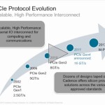
Today Cadence announced a collaboration with Mellanox Technologies to demonstrate multi-lane interoperability between Mellanox’s physical interface (PHY) IP for PCIe 4.0 technology and Cadence’s 16Gbps multi-link and multi-protocol PHY IP implemented in TSMC’s 16nm FinFET Plus (16FF+) process. Customers seeking to develop and deploy next-generation green data centers can now use a silicon-proven IP solution from Cadence for immediate integration and fastest market deployment. Cadence and Mellanox are scheduled to demonstrate electrical interoperability for PCIe 4.0 architecture between their respective PHY solutions at the 2016 TSMC Symposium on March 15, 2016 in Santa Clara, California.