Intel’s next-generation “Ivy Bridge” chips will include a host of improvements, including integrated graphics that the company claims will narrow the lead now held by AMD’s Fusion APUs.
I expect that that gap, from everything that I’ve seen, is closing fast,” Intel’s director of graphics architecture Tom Piazza told an Ivy Bridge confab on Tuesday at the Intel Developer Forum (IDF), when he was asked if Intel was closing the performance gap with its competition – presumably AMD. “I don’t see any reason why it won’t close all the way,” he confidently continued, “and maybe you’ll be asking the other guys that question in a year or two.”
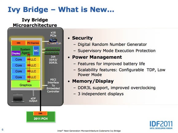
Improved graphics performance is not the only architectural improvement in Ivy Bridge over Intel’s current “Sandy Bridge” chips. Also new, said Ivy Bridge interconnect and integration engineer Varghese George at the same session, are support for low-power DDR3L memory, dynamic (no reboot) overclocking control of both the compute and graphics cores, power-management improvements, security enhancements to guard against escalation of privilege attacks, and more.
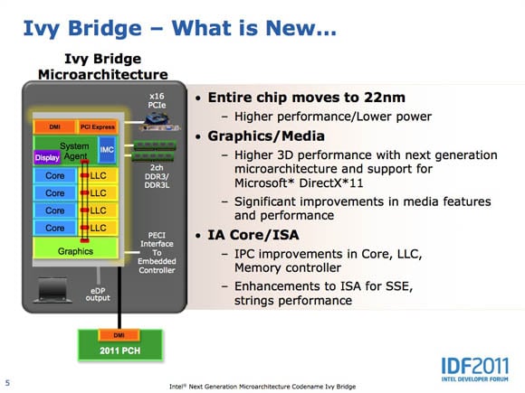
 Ivy Bridge is not just a shrink of Sandy Bridge from 32nm to 22nm …
 … it includes improvements to a host of architectural improvements, as well
Such a significant redesign is unusual in Intel’s “tick-tock” chip-release cadence, in which a tick in a process shrink – say, from 32nm to 22nm – and a tock is a new architecture. During his IDF keynote on Wednesday, Intel’s PC client honcho Mooly Eden referred to Ivy Bridge as “a tick-plus” – a scaled-down version of Sandy Bridge, but with its own architectural improvements.
Eden focused on one of those improvements, a power-saving enhancement called power-aware interupt routing, or PAIR, which intelligently sends interrupts to cores that are already up and running, rather than to those that have been powered down and are comfortably asleep.
Accessories and external devices continually send interrupts to a CPU to check on what’s what. USB, for example sends around three thousand interrupts per second – and if a core is asleep, it must wake up to handle that interrupt before it can go back to sleep.
“And the minute it wakes up, it starts consuming power,” Eden explained, “and it tries to go back to sleep and [the interrupt] wakes it up – and you know how annoying it is when you wake up and sleep and wake up and sleep.”
Without PAIR, Mooley said, each of USB’s 3,000 interrupts per second are sent to core 0 – and if core 0 is asleep, USB wakes it up, which wastes power. Simply put, PAIR routes interrupts to a core that’s already awake, thus saving power. A small amount, to be sure, but in the world of power management, many small amounts can add up to significant power savings.
Greased graphics turn a tick into a tock
But it’s the improvements to Ivy Bridge’s graphics improvement that both Mooley and Piazza cited as the main reason that Ivy Bridge should be considered a “tick-plus”.
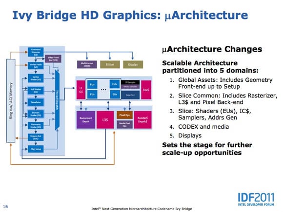
 The graphics elements in Ivy Bridge have been reshuffled and enhanced for better performance (click to enlarge)
Ivy Bridge’s integrated graphics, Piazza said, “is not a tick, it’s a tock,” citing such improvements as support for DirectX 11 – in AMD’s APUs, but new for Intel – plus improved media performance and the ability to drive three displays from one Ivy Bridge chip, or two when a laptop is docked with its lid closed.
“So now you can dock with your lid down,” Piazza said, “and those people with three eyes or three heads, you can also have three displays if you keep your lid up.”
In addition to enabling Cerberus to better enjoy his Ivy Bridge Ultrabook™, the new graphics architecture, Piazza said, is able to “fix some things that were less efficient on Sandy Bridge, and create a system that’s much more scalable, much more optimal” when used in different chips in the Ivy Bridge series.
The Ivy Bridge design team reordered the graphics pipeline, partially to make it more scalable through the addition of more or fewer graphics processing units, and partially to simply make it faster and more efficient.

They also added an L3 cache deep inside the graphics goodness. “In Sandy Bridge,” Piazza said, “we were going to put an L3 cache in. We did not do it because we couldn’t find any real performance reason to do it.” Asked why not, he answered, speaking of the Sandy Bridge development process: “If you look into Sandy Bridge, you can almost turn the L3 off – you’ll see very few applications that suffer, and they suffer in the range of 5 to 10 per cent.”
The bottom line: “There was no performance to be gained from the L3, at the time, so we just killed it.”
In the new, rearranged Ivy Bridge graphics architecture, however, the L3 is closer to the units that it needs to feed, and it conserves power “because you don’t have to go out and light up the whole [cache communications] ring,’ which would eat put more power and eat up bandwidth.” The addition of the L3 in Ivy Bridge “just floats all boats,” Piazza said.
Piazza also ran down a laundry list of architectural changes and improvements in Ivy Bridge, including shared local memory. “You take a look at what we did here – the amount of scatter-gathers per clock – is 32 times more than Sandy Bridge. If you’re running GPGPU workloads … don’t be surprised if performance is extremely higher,” he said, citing 20X improvements they’ve seen in some workloads.
He also pointed out other improvements, such as better geometry performance, buffer-clearing optimizations using scoreboarding, higher sampler throughput, higher – and more honest – peak gigaflops, and improved anisotropic performance. “For those people who have been looking at our anisotropic angle thing,” he said, “we now draw circles instead of flower petals.”
Toss in a few more upgrades – such as the ability to support both encoding and decoding stereoscopic 3D – and the tick-tock, tick-plus cadence packed inside Ivy Bridge’s 1.48bn transistors might be the sound of stopwatch timing AMD and Intel in the on-die, integrated-graphics race. ®
This article originally appeared in The Register. It appears here in its entirety as part of a cross-publishing agreement.


