
Benjamin Levine, Associate Professor, Department of Chemistry, Michigan State University.
Researchers are using XSEDE supercomputers to develop better semiconductors for solar engery. In this TACC Podcast, host Jorge Salazar interviews Benjamin Levine, an associate professor in the Department of Chemistry at Michigan State University. Dr. Levine models the behavior caused by defects in materials, such as doping bulk silicon to transform it into semiconductors in transistors, LEDs, and solar cells.
Levine and his team have used over 975,000 compute hours on the Maverick supercomputer, a dedicated visualization and data analysis resource architected with 132 NVIDIA Tesla K40 “Atlas” GPUs for remote visualization and GPU computing to the national community.
Solar cells have a problem with heat. Photovoltaics on solar panels lose some energy as heat in when they convert sunlight to electricity. The reverse holds true for LED lights, which convert electricity into light.
Scientists call the heat loss in LEDs and solar cells “non-radiative recombination.” And they’ve struggled to understand the basic physics of this heat loss, especially for materials with molecules of over 20 atoms.
“The real challenge here is system size,” explained Ben Levine, associate professor in the Department of Chemistry at Michigan State University. “Going from that 10-20 atom limit up to 50-100-200 atoms has been the real computation challenge here,” Levine said. That’s because the calculations involved scale with the size of the system to some power, sometimes four or up to six, Levine said. “Making the system ten times bigger actually requires us to perform maybe 10,000 times more operations. It’s really a big change in the size of our calculations.”
Levine’s calculations involve a concept in molecular photochemistry called a conical intersection – points of degeneracy between the potential energy surfaces of two or more electronic states in a closed system. A perspective studypublished September of 2017 in the Journal of Physical Chemistry Letters found that recent computational and theoretical developments have enabled the location of defect-induced conical intersections in semiconductor nanomaterials.
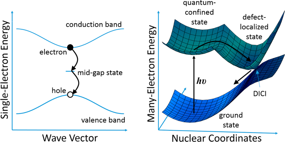
Illustrations of the midgap state picture of recombination (left) and the DICI picture (right). Key differences include the consideration of correlated many-electron states and nuclear motion in the DICI picture. Credit: Ben Levine.
The key contribution of our work has been to show that we can understand these recombination processes in materials by looking at these conical intersections,” Levine said. “We’ve been able to show is that the conical intersections can be associated with specific structural defects in the material.”
The holy grail for materials science would be to predict non-radiative recombination behavior of a material based on its structural defects. These defects come from ‘doping‘ semiconductors with impurities to control and modulate its electrical properties.
Read the Full Story * Download the MP3
Sign up for our insideHPC Newsletter