![]() CEA, the French Atomic Energy and Alternative Energy Commission, today presented what it said is a path to European exascale supercomputing utilizing technologies that combine “finer 3D interconnect paths for greater bandwidth between chiplets” within heterogenous nodes made up of generic processors.
CEA, the French Atomic Energy and Alternative Energy Commission, today presented what it said is a path to European exascale supercomputing utilizing technologies that combine “finer 3D interconnect paths for greater bandwidth between chiplets” within heterogenous nodes made up of generic processors.
In an invited paper released at the IDEM 2020 (International Electron Devices Meeting) conference in San Francisco, CEA said its approach improves peak performance through “co-optimization of advanced integration technologies with disruptive architectures.” It “…demonstrate(s) the benefit of new integration methods and processes following two main paths: finer 3D interconnect pitches, leading to improved bandwidth between compute chiplets, and assembly technologies that allow increasing heterogeneity in packaging.”
“These R&D successes open a path towards heterogeneous processors that will enable exascale-level supercomputers,” said Denis Dutoit, lead author of the paper (located here, available to IDEM registrants) and scientist at CEA-List, an institute within CEA’s R&D unit, CEA Tech. “We demonstrated that co-optimization of advanced architectures with 3D integration technologies achieves the level of computing performance and bandwidth required for HPC.”
This research work was funded by the French National Programme d’Investissements d’Avenir (Investments in the Future), IRT Nanoelec and was supported by the ExaNoDe project, (European Exascale Processor & Memory Node Design). In addition, CEA said in its announcement that “the importance of a 3D-integration solution to developing HPC processors is confirmed by the European Processor Initiative (EPI), with which CEA is deeply involved. Its aim is to design and implement a roadmap for a new family of low-power European processors for extreme scale computing, high-performance Big Data and a range of emerging applications.”
The effort fits with a global trend in which national and, in this case, regional efforts to build exascale-class systems based on processors they’ve developed themselves. This has been widely noted by industry observers, including Steve Conway, senior advisor for HPC market dynamics at HPC industry analyst firm Hyperion Research. “Governments around the world have recognized that HPC is not just for science but it’s crucial for economic competitiveness,” he recently told us. “That recognition is what has allowed all these huge sums to be made available for exascale systems. On the other hand, it’s also led to the disruption of the market – the indigenous technology movements in China, Japan and Europe – because if it’s so strategic the countries don’t want to be reliant on foreign vendors. So there’s this big push to develop indigenous supply chains and technologies.”
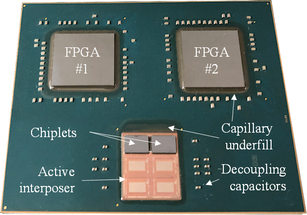
ExaNoDe heterogeneous multi-chip module (source: CEA)
CEA said its paper shows that the architecture developed by CEA List, co-optimizing a 3D toolbox developed by CEA Leti (the CEA Tech research unit for micro- and nanotechnologies) for mixing intra- and inter-layer interconnects and assembly technologies, enables higher bandwidth and heterogeneity for HPC processors.
“Because chiplets stacked on active interposer allow modularity and reusability at low development costs, CEA List also is investigating using this new methodology for HPC architectures in the embedded world, for compute-intensive accelerators,” CEA said. “For edge applications requiring a high level of computation and memory, such as artificial intelligence, chiplet-based partitioning will enable the creation of a broad range of solutions to meet the needs for embedded AI. Potential uses include autonomous driving, transport applications and industry 4.0.”
The organization said current CEA Leti research addresses die-to-wafer direct hybrid-bonding technology, which it said offers denser 3D interconnects with better electrical, mechanical and thermal parameters, and allows ultra high-bandwidth capabilities in heterogeneous systems. “CEA Leti also is working on high-density through silicon vias (TSV) (pitch 1 to 4 µms) to create together with die-to-wafer hybrid bonding a complete dense 3D stack. For the longer term, CEA Leti is also investigating innovative photonic-interposer technology as a 3D-based photonic chiplet approach to enable interconnection of tens of computing chiplets with the resulting chip-to-chip communication bandwidth, latency and energy.”