 New Intel CEO Pat Gelsinger delivered an upbeat corporate update this afternoon in the form of a webinar that emphasized Intel’s integrated device manufacturing, “IDM.2.0” strategy for manufacturing and product development that combines the company’s internal network of factories with third-party outsourced capacity and new Intel foundries in the U.S. and Europe.
“As I hope you’ve gathered, Intel is back,” Gelsinger said near the end of his hour-long remarks. “The old Intel is now the new Intel.”
Highlights of Gelsinger’s remarks included:
- Announcing manufacturing expansion plans beginning with about a $20 billion investment to build two new fabs in Arizona.
- Intel 7 nanometer process development progress with tape in of 7nm compute tile for “Meteor Lake” expected in the second quarter of 2021.
- Announcing Intel Foundry Services with plans to become a provider of foundry capacity in the U.S. and Europe to serve customers globally.
- Announcing plans for new research collaboration with IBM.
- Resuscitation of the old Intel Developer Forum with Intel On, to be held in San Francisco in October.
“We are setting a course for a new era of innovation and product leadership at Intel,” said Gelsinger. “Intel is the only company with the depth and breadth of software, silicon and platforms, packaging, and process with at-scale manufacturing customers can depend on for their next-generation innovations. IDM 2.0 is an elegant strategy that only Intel can deliver – and it’s a winning formula. We will use it to design the best products and manufacture them in the best way possible for every category we compete in.”
On the topic of 7nm process chips, in which rival AMD has stolen a march on Intel with its recently released “Milan” EPYC 7300 CPU, Intel said, “The company’s 7nm development is progressing well, driven by increased use of extreme ultraviolet lithography (EUV) in a rearchitected, simplified process flow. Intel expects to tape in the compute tile for its first 7nm client CPU (code-named “Meteor Lake”) in the second quarter of this year. In addition to process innovation, Intel’s leadership in packaging technology is an important differentiator that enables the combination of multiple IPs or ’tiles’ to deliver uniquely tailored products….”
A theme running through Gelsinger’s remarks is his determination to instill an ethic of fulfilling or exceeding expectations, a veiled reference to data center server CPUs and GPUs that have missed launch dates – products with direct bearing on Intel’s HPC customers.

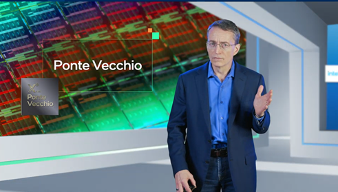
Intel CEO Pat Gelsinger speaking today
“We’re going to work hard to always be on the front foot of the technology, of the capacity, and overachieving on every aspect of our businesses as we look forward,” Gelsinger said. “I’ll say one of the themes to my young CEO tenure: ‘Execute, execute, execute.’ We’re bringing back the execution discipline of Intel, I’ve called it the ‘Grovian culture,’ (referring to former Intel CEO Andy Grove) that we do what we say what we’re going to do, we have that confidence in our execution, that our teams are fired up, when we say we’re going to do X we’re going to do 1.1x every time that we make a commitment. That’s the Intel culture that we are bringing back.”
Executing on that ethic would be welcomed by Argonne National Laboratory, which had expected delivery this year of the country’s first exascale supercomputer, Aurora, for which Intel is the prime contractor. But delays in the shipment of the 7nm “Ponte Vecchio” GPU, to be implemented in the Aurora, has caused Aurora’s ship date to be pushed out until next year.
Without mentioning a specific Ponte Vecchio timetable, Gelsinger made positive comments about the GPU, saying, “Ponte Vecchio is excellent demonstration of our ability to combine multiple process technologies both internal and external, with novel packaging technology to uniquely tailor products to customer’s markets and needs. It uses more than 40 different tiles integrated into a single package. This package is a diverse combination of more than 100 billion transistors manufactured in multiple process technologies.”
Holding a prototype of the chip, Gelsinger said, “13 years ago, IBM introduced the world’s first petaflop supercomputer, which filled an entire, very large room. Now, right here in my hand, I have a petaflop-scale AI computer easily accessible to developers….
Gelsinger said Intel’s $20B fab build-out will create over 3,000 high tech jobs, more than 3,000 construction jobs and approximately 15,000 local long-term jobs. He said the company plans to announce the next phase of capacity expansions in the U.S., Europe and other global locations within the year.
Intel also said it “plans to engage the technology ecosystem and industry partners to deliver on its IDM 2.0 vision.” To that end, Intel and IBM today announced plans for a research collaboration focused on next–generation logic and packaging technologies. “Leveraging each company’s capabilities and talent in Hillsboro, Oregon, and Albany, New York, this collaboration aims to accelerate semiconductor manufacturing innovation across the ecosystem, enhance the competitiveness of the U.S. semiconductor industry and support key U.S. government initiatives,” Intel said today.


