![]() IBM today unveiled what it said is the first chip with 2 nanometer (nm) nanosheet technology. Though still more than two years away from going into production, the company said the 2nm chip will be used to power devices ranging from cell phones to HPC-class data center servers and will deliver nearly 50 percent higher performance, or 75 percent lower energy use, compared with today’s most powerful 7nm chips.
IBM today unveiled what it said is the first chip with 2 nanometer (nm) nanosheet technology. Though still more than two years away from going into production, the company said the 2nm chip will be used to power devices ranging from cell phones to HPC-class data center servers and will deliver nearly 50 percent higher performance, or 75 percent lower energy use, compared with today’s most powerful 7nm chips.
IBM said the potential benefits of 2nm chips include cutting carbon footprints of data centers (1 percent and growing of global energy use), along with – among other examples – extending cell phone battery charges, improving laptop capabilities and accelerating autonomous vehicle object detection.
“nm,” an abbreviation for nanometer, is one billionth of a meter, also expressed as 0.000000001 or 10-9 meters (for perspective, hair grows at roughly 1 nm/second). In chip design, “nm” is a measure of the length of a transistor gate – the smaller the gate the more processing power that can be packed into a given space, resulting in greater density and efficiency.
Though better known for other aspects of technology, IBM is active in the chip category. The company’s semiconductor legacy includes early implementation of 7nm and 5nm process technologies, single cell DRAM, the Dennard Scaling Laws, chemically amplified photoresists, copper interconnect wiring, silicon on insulator technology, multi core microprocessors, High-k gate dielectrics, embedded DRAM and 3D chip stacking. IBM’s first commercialized offering, including IBM 7nm advancements, are scheduled for debut later this year in IBM POWER10-based IBM Power Systems.
While respected in tech circles, IBM’s POWER chips have met with limited commercial success. POWER CPU coupled with Nvidia GPUs are used in two of the world’s three most powerful supercomputers, DOE’s Summit and Sierra HPC systems housed at Oak Ridge and Lawrence Livermore national laboratories, respectively. Those and other POWER-Nvidia powered servers served as pathfinders for what is now a widely accepting architectural model for HPC-class servers coupling CPUs and GPUs. But IBM’s POWER product line has not attained the company’s ambitious market adoption goals.
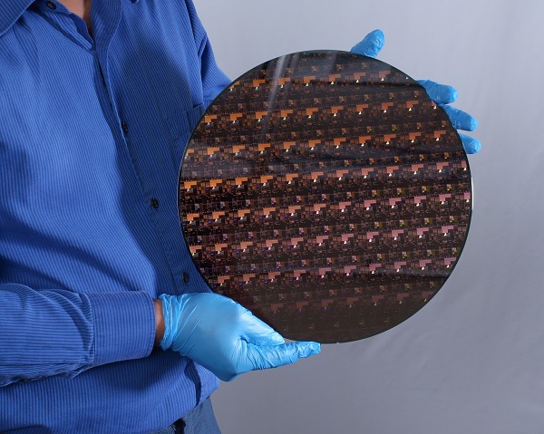
A 2 nm wafer fabricated by IBM Research containing hundreds of chips. Courtesy of IBM Research.
“The IBM innovation reflected in this new 2nm chip is essential to the entire semiconductor and IT industry,” said Darío Gil, SVP and director of IBM Research. “It is the product of IBM’s approach of taking on hard tech challenges and a demonstration of how breakthroughs can result from sustained investments and a collaborative R&D ecosystem approach.”
IBM semiconductor development is based at its research lab at the Albany Nanotech Complex in Albany, NY, where IBM scientists work with public and private sector partners on logic scaling and semiconductor capabilities. The 2 nm design is based on IBM’s nanosheet technology and will allow the 2 nm chip to fit up to 50 billion transistors on a chip the size of a fingernail, according to IBM.