
CEO Pat Gelsinger at today’s Intel Accelerated
Intel Corporation today announced a detailed process and packaging technology roadmaps of “foundational innovations” for products through 2025 and beyond.
In addition to announcing RibbonFET, its first new transistor architecture in more than 10 years, and PowerVia, a backside power delivery method, the company highlighted its planned adoption of next-generation extreme ultraviolet lithography (EUV), referred to as High Numerical Aperture (High NA) EUV. Intel said it is positioned to receive the first High NA EUV production tool in the industry.
In response to what it said is growing recognition that that traditional nanometer-based process node naming no longer matches the actual gate-length metric, Intel introduced a new naming structure for its process nodes, “creating a clear and consistent framework to give customers a more accurate view of process nodes across the industry.”
This clarity, the company said, takes on more significance with the launch of Intel Foundry Services (IFS). “The innovations unveiled today will not only enable Intel’s product roadmap; they will also be critical for our foundry customers,” said CEO Pat Gelsinger. “The interest in IFS has been strong and I’m thrilled that today we announced our first two major customers.”
Intel technologists described the following roadmap with the new node names and technologies enabling each node:
- Intel 7 delivers an approximately 10 to 15 percent performance-per-watt increase versus Intel 10nm SuperFin, based on FinFET transistor optimizations. Intel 7 will be featured in products such as Alder Lake for client in 2021 and Sapphire Rapids for the data center, which is expected to be in production in the first quarter of 2022.
- Intel 4 utilizes EUV lithography to print small features using ultra-short wavelength light. With a roughly 20 percent performance-per-watt increase, along with area improvements, Intel 4 will be ready for production in the second half of 2022 for products shipping in 2023, including Meteor Lake for client and Granite Rapids for the data center.
- Intel 3 leverages further FinFET optimizations and increased EUV to deliver an approximately 18 percent performance-per-watt increase over Intel 4, along with additional area improvements. Intel 3 will be ready to begin manufacturing products in the second half of 2023.
- Intel 20A begins what the company called “the angstrom era” with two technologies, RibbonFET and PowerVia. RibbonFET, Intel’s implementation of a gate-all-around transistor, will be the company’s first new transistor architecture since FinFET in 2011. Intel said the technology delivers faster transistor switching speeds while achieving the same drive current as multiple fins in a smaller footprint. PowerVia is Intel’s implementation of backside power delivery, optimizing signal transmission by eliminating the need for power routing on the front side of the wafer, Intel said. Intel 20A is expected to ramp in 2024. The company said it partnering with Qualcomm using its Intel 20A process technology.
- 2025 and beyond: Beyond Intel 20A, Intel 18A is in development for early 2025 with refinements to RibbonFET designed to deliver an increase in transistor performance. Intel is also working on next-gen High NA EUV, and expects to receive the first production tool in the industry. Intel is partnering with ASML in this technology.
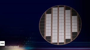
A test package of “Meteor Lake” with Foveros wafer-level assembly
“We led the transition to strained silicon at 90nm, to high-k metal gates at 45nm and to FinFET at 22nm,” said Dr. Ann Kelleher, SVP/GM of Technology Development. “Intel 20A will be another watershed moment in process technology with two groundbreaking innovations: RibbonFET and PowerVia.”
Intel announced that AWS will be the first customer to use IFS packaging solutions, while also providing the following insights into the company’s industry-leading advanced packaging roadmap:
- EMIB is the first 2.5D embedded bridge solution, according to Intel, with products shipping since 2017. Sapphire Rapids will be the first Intel Xeon data center product to ship in volume with EMIB (embedded multi-die interconnect bridge). It will also be the first dual-reticle-sized device, delivering nearly the same performance as a monolithic design, the company said. Beyond Sapphire Rapids, the next generation of EMIB will move from a 55-micron bump pitch to 45 microns.
- Foveros leverages wafer-level packaging capabilities to provide a 3D stacking solution. Meteor Lake will be the second-generation implementation of Foveros in a client product and features a bump pitch of 36 microns, tiles spanning multiple technology nodes and a thermal design power range from 5 to 125W.
- Foveros Omni is in the next generation of Foveros technology, providing unbounded flexibility with performance 3D stacking technology for die-to-die interconnect and modular designs. Foveros Omni allows die disaggregation, mixing multiple top die tiles with multiple base tiles across mixed fab nodes and is expected to be ready for volume manufacturing in 2023.
- Foveros Direct moves to direct copper-to-copper bonding for low-resistance interconnects and blurs the boundary between where the wafer ends and where the package begins. Foveros Direct enables sub-10-micron bump pitches, “providing an order of magnitude increase in the interconnect density for 3D stacking, opening new concepts for functional die partitioning that were previously unachievable,” Intel said. Foveros Direct is complementary to Foveros Omni and is also expected to be ready in 2023.
Intel said the technologies discussed today were primarily developed at Intel’s facilities in Oregon and Arizona, drawing on collaboration with an ecosystem of partners in the U.S. and Europe.
The company closed its webcast by confirming more details on its Intel InnovatiON event. Intel InnovatiON will be held in San Francisco and online on Oct. 27-28, 2021. More information is available at the Intel ON website.
For more information on Intel’s process roadmap and node naming, visit the process factsheet. A replay of today’s webcast is at Intel Newsroom.