
Intel’s Raja Koduri
Harried data center and HPC server market dominator Intel today unveiled what the company said is its biggest shifts in Intel architectures in a generation.
The Architecture Day event included looks at the two chips that will power the delayed Aurora exascale supercomputer, to be installed at Argonne National Laboratory; those chips are: Sapphire Rapids, Intel’s new (and delayed) x86 data center architecture with Performance-core and various accelerator engines, and Ponte Vecchio, Intel’s delayed data center GPU architecture, which Intel said has its highest ever compute density.
Regarding Ponte Vecchio’s status, Intel said the chip “is powered on, is in validation and has begun limited sampling to customers. Ponte Vecchio will be released in 2022 for HPC and AI markets.”
“Today, we unveiled our biggest shifts in Intel architectures in a generation,” said Raja Koduri, SVP/GM of Intel’s Accelerated Computing Systems and Graphics Group. “This includes … Sapphire Rapids, Intel’s new standard-setting data center architecture with our new Performance-core and various accelerator engines… and Ponte Vecchio, our tour-de-force data center GPU architecture with Intel’s highest ever compute density.”
Starting with Intel’s Xeon Scalable Sapphire Rapids CPU, the company said the chip “represents Intel’s biggest data center platform…,” and is “workload-optimized to deliver high performance on elastic compute models like cloud, microservices and AI.”
“At the heart of Sapphire Rapids is a tiled, modular SoC architecture that leverages Intel’s embedded multi-die interconnect bridge (EMIB) packaging technology to deliver significant scalability while maintaining the benefits of a monolithic CPU interface,” the company said. “Sapphire Rapids provides a single balanced unified memory access architecture, with every thread having full access to all resources on all tiles, including caches, memory and I/O. The result offers consistent low-latency and high cross-section bandwidth across the entire SoC.”

Sapphire Rapids is built on Intel 7 process technology. The new acceleration engines include:
- The Intel Accelerator Interfacing Architecture (AIA), designed to support efficient dispatch, synchronization and signaling to accelerators and devices.
- Intel’s Advanced Matrix Extensions (AMX) is a workload acceleration engine introduced in Sapphire Rapids that Intel said delivers massive speed-up to the tensor processing at the heart of deep learning algorithms, delivering boosts in compute power with 2K INT8 and 1K BFP16 operations per cycle. Using early Sapphire Rapids silicon, optimized internal matrix-multiply micro benchmarks run over 7x faster using AMX instruction set extensions compared to a version of the same micro benchmark using Intel AVX-512 VNNI instructions, according to the company.
- Intel’s Data Streaming Accelerator (DSA) is designed to offload common data movement tasks that cause overhead in data center scale deployments, improving “processing of these overhead tasks to deliver increased overall workload performance and can move data among CPU, memory and caches, as well as all attached memory, storage and network devices… The processor is built to drive industry technology transitions with advanced memory and next-generation I/O, including PCIe 5.0, CXL 1.1, DDR5 and HBM technologies,” the company said.
Regarding the Ponte Vecchio GPU, Intel said it is based on the Xe HPC microarchitecture and incorporates compute density to accelerate AI, high performance computing (HPC), and advanced analytics workloads. Intel disclosed IP block information of the Xe HPC microarchitecture; including eight vector and matrix engines (referred to as XMX – Xe Matrix eXtensions) per Xe-core; slice and stack information; and tile information, including process nodes for the compute, base, and Xe Link tiles.
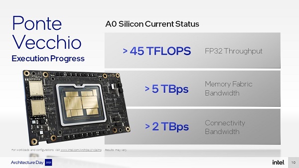
“Intel’s A0 silicon performance is providing greater than 45 TFLOPS FP32 throughput, greater than 5 TBps memory fabric bandwidth and greater than 2 TBps connectivity bandwidth,” the company said.
Intel also shared a demo showing ResNet inference performance of over 43,000 images per second and greater than 3,400 images per second with ResNet training, “both of which are on track to deliver performance leadership,” the company said.
Ponte Vecchio is comprised of several designs that manifest in tiles, which are then assembled through an EMIB tile that enables a low-power, high-speed connection between the tiles. These are put together in Foveros packaging that creates the 3D stacking of active silicon for power and interconnect density. A high-speed MDFI interconnect allows scaling from one to two stacks.
Compute Tile is a dense package of Xe-cores and is the heart of Ponte Vecchio. Intel said one tile has eight Xe-cores with a total of 4MB L1 cache, its key to delivering power-efficient compute and is built on TSMC’s advanced process technology, N5. The tile has a tight 36-micron bump pitch for 3D stacking with Foveros.
Base Tile is the “connective tissue” of Ponte Vecchio and is a large die built on Intel 7 optimized for Foveros technology. The Base Tile is where complex I/O and high bandwidth components come together with the SoC infrastructure – PCIe Gen5, HBM2e memory, MDFI links to connect tile-to-tile and EMIB bridges. Supporting its role as an “infinite connectivity machine,” Base Tile has “super-high-bandwidth 3D connect with high 2D interconnect and low latency.
Xe Link Tile provides connectivity between GPUs supporting eight links per tile and is critical for scale-up for HPC and AI, targeting the fastest SerDes supported at Intel – up to 90G. The tile was added to enable the scale-up solution for the Aurora exascale supercomputer