![]() Today, IBM and Samsung Electronics jointly announced what they said is a breakthrough in semiconductor design utilizing a new transistor architecture that allows more transistors to be packed in an IC chip. The key: the transistors stand up rather than lie down, thus taking up less space and offering “a pathway to the continuation of Moore’s Law,” IBM said.
Today, IBM and Samsung Electronics jointly announced what they said is a breakthrough in semiconductor design utilizing a new transistor architecture that allows more transistors to be packed in an IC chip. The key: the transistors stand up rather than lie down, thus taking up less space and offering “a pathway to the continuation of Moore’s Law,” IBM said.
![]()
Transistors have historically been built to lie flat upon the surface of a semiconductor, with the electric current flowing laterally through them. This is called lateral-transport field effect transistors (FETs), such as fin field effect transistor, or finFET (which got its name because silicon body resembles the back fin of a fish), which layers transistors along a wafer’s surface. Vertical Transport Field Effect Transistors (VTFET), on the other hand, layer transistors perpendicular to the silicon wafer and directs current flow vertical to the wafer surface.
The result, according to the companies: the VTFET process extends Moore’s Law as chip designers attempt to pack more transistors into a fixed space.
“This new approach addresses scaling barriers by relaxing physical constraints on transistor gate length, spacer thickness, and contact size so that these features can each be optimized; either for performance or energy consumption,” stated IBMers Brent Anderson (VTFET architect and program manager) and Hemanth Jagannathan (VTFET hardware technologist and principal research staff member).
VTFET also influences the contact points for the transistors, allowing for greater current flow with less wasted energy. Overall, IBM and Samsung said, “the new design aims to deliver a two times improvement in performance or an 85 percent reduction in energy use as compared to scaled finFET alternatives.”
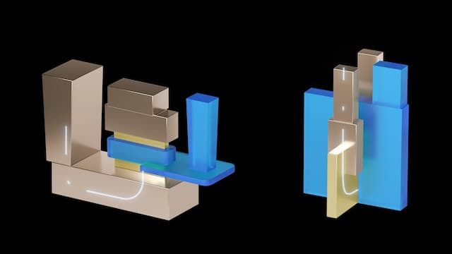
Transistor comparison: VTFET (left) and lateral FET with current flowing through them
The technique was developed at the SUNY Polytechnic Institute’s Albany Nanotech Complex in New York, a facility focused on semiconductor research and prototyping. IBM said R&D at the complex is often directed at commercialization, and on that end of the chip lifecycle today IBM and Samsung also announced that Samsung will manufacture IBM’s chips at the 5 nm node and expected to be used in IBM’s server platforms.
In their blog, Anderson and Jagannathan explained that designers have customarily pack more transistors onto a chip by shrinking its gate pitch and wiring pitch. “The physical space where all the components fit is called the Contacted Gate Pitch (CGP). The ability to shrink gate and wiring pitches has allowed integrated-circuit designers to go from thousands to millions to billions of transistors in our devices. But with the most advanced finFET technologies, there’s only so much room for spacers, gates and contacts. Once you’ve reached the CGP limit, you’re out of space.
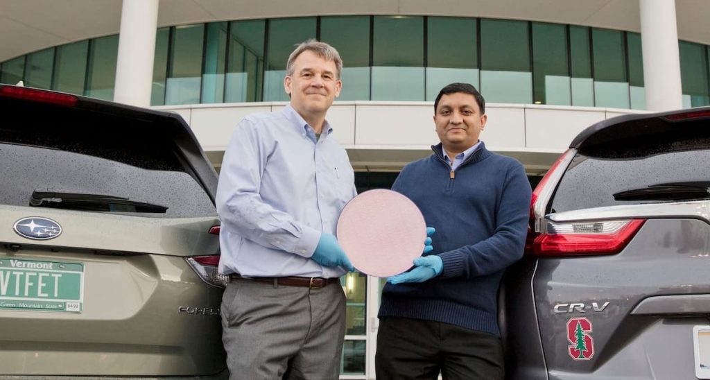
IBMers Brent Anderson and Hemanth Jagannathan holding a wafer outside their lab
“By orienting electrical current flow vertically, the gates, spaces and contacts are no longer constrained in traditional ways: We have room to scale CGP while maintaining healthy transistor, contact, and isolation (spacer and shallow trench isolation, STI) size. Released from the constraints of the lateral layout and current flow, we were able to use larger source/drain contacts to increase the current on the device. The gate length can be selected to optimize device drive current and leakage, while the spacer thickness can be independently optimized for lower capacitance. We are no longer forced to tradeoff the gate, spacer, and contact size, which can result in improved switching speed and reduced power use.”
Today’s announcement follows Samsung’s 2018 agreement to manufacture IBM’s 7 nm chips, which became available in IBM Power10 servers earlier this year. The IBM Telum processor, also revealed earlier this year, is similarly manufactured by Samsung using IBM’s designs.
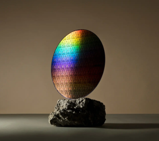
A VTFET wafer
IBM said the vertical transistor architecture could deliver significant improvements, including:
- Potential device architecture that enables semiconductor device scaling to continue beyond nanosheet.
- Cell phone batteries that could go over a week without being charged, instead of days.
- Energy intensive processes, such as cryptomining and data encryption, could require significantly less energy with smaller carbon footprint.
- Expansion of Internet of Things (IoT) and edge devices with lower energy needs, allowing them to operate in more diverse environments like ocean buoys, autonomous vehicles, and spacecraft.