 [SPONSORED CONTENT] “FLOPS are cheap, moving data is expensive.” In HPC circles this sentiment is heard often. There’s a growing sense that classical HPC systems and the advanced chips that power them are pushing up against their practical limits, that some foundational new technology is needed to build more balanced systems to achieve the next major advance in supercomputing power.
Central to this sense is connectivity. Processing, memory, storage – their power and capacity continue to grow. But electrical I/O interconnect bandwidth, while also expanding, isn’t keeping pace.
The problem is widely recognized in HPC. But solving the problem by moving to a new and superior interconnect technology, that’s only begun to happen at research labs and tech companies.
Moving past electrical I/O was the topic of a fascinating session at SC22 last month in Dallas entitled “Transforming the Future of HPC with Silicon Photonics, ” with panelists from Lawrence Berkeley National Laboratory, Columbia University, NVIDIA, Ayar Labs, the Defense Advanced Research Projects Agency (DARPA), the Department of Energy’s (DOE) Office of Advanced Scientific Computing Research, Intel and the University of Southern California.
As the title suggests, silicon photonics holds the promise of major HPC-class server performance gains combined with significantly lower power consumption. Panelist and optical I/O advocate Fabrizio Petrini, senior principal engineer at Intel Labs, noted that there continues to be skepticism about silicon photonics in the HPC community and that more development work remains before broad adoption can take place.
“But there are some things that are on our side,” he said. “For example, copper is finally reaching a limit. Very smart people are trying to push electrical technology, but … they’re not finding enough solutions. They’re getting to a point, you can tell from the tone of the voice and the tone at meetings, there’s a level of desperation, that they have a problem.”
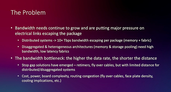
Mark Wade, CTO, SVP of engineering and co-founder of silicon photonics startup Ayar Labs, began his session remarks with a series of problem statements, among them: “Bandwidth needs continue to grow and are putting major pressure on electrical links escaping the package.”
For some of today’s distributed systems, he said, 10-plus terabytes/second of bandwidth are escaping per package, and disaggregated and heterogeneous architectures that utilize memory and storage pooling put tremendous bandwidth and latency demands on fabrics.
source: Ayar Labs
In the face of these pressures, Wade said designers of advanced chips used in HPC-class servers have resorted to stop-gap measures to expand bandwidth, including copper fly-over cables and retimers. But these introduce new sets of problems: higher costs, hotter chips and systems requiring more power consumption, extreme board density and board complexity, and routing congestion.
“It’s a bandwidth bottleneck…,” Wade said, “you’re really fighting physics all along the way.”
“We’re finally getting to the point where there’s a customer or a market with a large enough pain point that can overcome the ‘Gee, it’s not an Ethernet transceiver’ aspect of this,” said Larry Dennison, NVIDIA’s director of network research. “It’s really taken us a while to recognize we’re going to hit a wall, the nature of the wall is cost and bandwidth, it’s finally become more clear to us. And certainly, internally to NVIDIA we recognize this and we’re investing heavily in silicon photonics.”
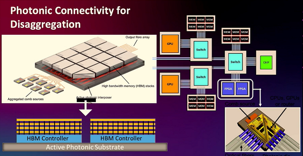
Silicon photonics offers the promise not only of significantly higher data transfer speeds but also reduced energy consumption. Another attractive characteristic: its lightning fast performance can traverse long and short distances – what the panelists called “distance independence.” And this, in turn, leads to thoughts of optical I/O as an enabler for a new era in HPC: just as electrical I/O has pushed the industry into the dense and hot chips, systems, clusters and data centers of today, silicon photonics could unlock entirely new approaches to system architectures of the future.
“The distance doesn’t matter,” said panelist Rich Carlson, program manager in the DOE’s Advanced Scientific Computing Program Office. “Once we’re in the photonic range, we can start thinking about redoing our architectures; to be more disaggregated; to have memory, compute accelerators, different kinds of technologies linking with brand new kinds of technologies, like quantum. In this world, where we’re doing multiple technologies, multiple systems, and we’re bringing them all together because we have a photonic system that ties everything together.”
Panelist Keren Bergman, the Charles Batchelor Professor of Electrical Engineering at Columbia University, picked up on the theme.
source: Keren Bergman, Columbia University
“At the system level with photonics, we have this incredible bandwidth density, very low energy photonic I/O,” she said. “We can think about these new architectures, we can think about sending the data across the system with the same bandwidth that we currently have in the socket in the chip. And that really opens up for this community this potential for flattened architectures that are just not limited by the bandwidth.
“The key point,” she continued, “is that with photonics it’s essentially about distance independence. That’s the key thing…, we can send that data anywhere in the system with the same bandwidth and the same energy.”
Wade expanded on the idea.
“If we have an optical I/O fabric, what can we start doing with it? Well, the idea is that once you’re in the optical domain, you’re effectively ‘distance insensitive,’” he said. “So anywhere from centimeters to kilometers, the optical signal doesn’t really care how far you’re going along that distance. You can start to build architectures that look at flattening the access between things like compute nodes and memory pools. And you can use some of the fan-out capabilities that you get with optics and look at reducing the number of switching hops you have to go through to access resources. You can start to peel apart this dense integration that’s happening now, when everything’s electrical signaling. And you can say, let’s use the distance of optical I/O to actually solve some of these key bottlenecks.”
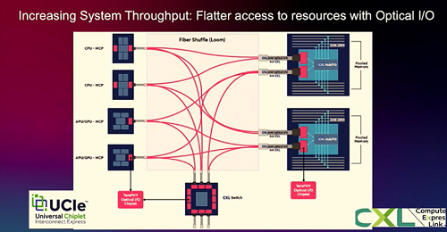
He envisioned a key role that could be played by CXL (Compute Express Link), the open standard for high-speed CPU-to-device and CPU-to-memory connections designed for data center servers.
source: Ayar Labs
“The idea is that you would have optical signals coming directly out of each of these little sockets, accessing pools of memory,” Wade said, referring to the nearby slide. “This example shows something like a CXL hub with I/O that’s connecting to these pools of memory. And then you also might go to CXL switches, but in a flatter kind of network topology.”

Ayar Labs’ Mark Wade
CXL raises an issue critical to silicon photonics’ future. Adoption of a new technology by the HPC industry requires open standards enabling its integration with incumbent components, and it takes an ecosystem. Look at the GPU. When NVIDIA helped build an early supercomputer (Titan, at Oak Ridge National Laboratory) combining GPUs with CPUs in 2010 and 2011, the company also supported the formation of an ecosystem. That ecosystem supported GPU-CPU integration as well as its optimization and commercialization, including financial backing, development of programming languages, training and services, complementary technologies, marketing and nurturing of a community of data scientists implementing machine learning applications. Eventually, GPU-based technology strategies and business models blossomed and became fully established.
By contrast, IBM labored for years to establish an HPC ecosystem centered on POWER processors and servers, but the ecosystem never quite reached critical mass, and by 2019, Big Blue had shifted away from the supercomputing systems business.
Something the optical I/O session at SC22 showed is that silicon photonics has the makings of an ecosystem. Not just venture-backed startups but also the big chip companies – Intel, NVIDIA and AMD – are actively developing the technology, mostly at the prototype phase. R&D is also happening at DOE’s national labs, at supercomputer research centers and in academia – such as the work Bergman and her team are doing at Columbia.
The case of Ayar Labs is instructive. The Silicon Valley company, founded in 2015, converts electrical signals from chips into speed-of-light optical signals. Its mission: full-fledged commercialization of an optical I/O chiplet. The company is led in part by former senior Intel execs, such as CEO Charlie Wuischpard, an HPC veteran who joined the company in 2018 and is steeped in the culture and methodologies of technology commercialization.
Ayar Labs’ TeraPHY optical I/O chiplet has been designed to be packaged alongside other chip companies’ compute tiles using open standards like CXL (see above) and UCIe, the Universal Chiplet Interconnect Express. At SC22, Ayar Labs presented a 2 Tbps full duplex working demonstration of their chiplet and SuperNova multi-wavelength laser.
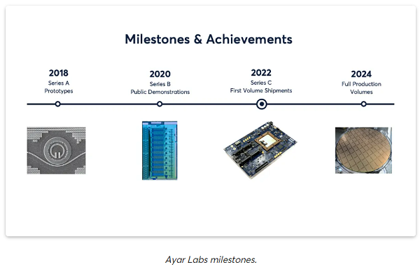
Here’s a series of Ayar Labs milestones as it moves toward full production volumes within the next couple of years.
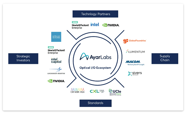
Ayar Labs was founded in part with an investment from Intel Capital, the company’s venture arm. Since 2015, the company has worked with GlobalFoundries on the GF Fotonix platform, a process optimized for photonics and electronics. The platform recently qualified for commercial readiness, which means it meets yield, process and reliability metrics and demonstrates process design kit (PDK) maturity.
The past year for Ayar Labs has seen announcements of partnerships and new customers, including a $130 million venture round, partnerships with HPE (see “HPE and Ayar Labs Partner to Bring Optical I/O to Slingshot Fabric for HPC and AI”) and with NVIDIA, a collaboration with Lockheed Martin, and a $15 million multi-year contract in support of the Department of Defense’s Project KANAGAWA.
All this activity has enabled Ayar Labs to assert that it has a two-year commercialization lead, supported by Wade with this slide from the SC22 session:
“Silicon photonics is at a point now that a big ecosystem is coming together to address our challenges in a volume manufacturable and scalable way,” said Wade. “So if you look at who we’re working with, look at who has invested in Ayar Labs and who our development partners are, we’ve invested all throughout the supply chain stack. Our view is that everyone has to come together and make a big ecosystem push to get these solutions actually pushed in volume out into the industry.”