HPC systems leader Hewlett Packard Enterprise and startup Ayar Labs, maker of chip-to-chip optical I/O connectivity, today announced a strategic collaboration to integrate silicon photonics within HPE’s high performance Slingshot fabric. Longer term, HPE envisions future generations of HPC systems interconnects significantly enhanced by optical I/O, which is a silicon photonics-based technology that uses light instead of electricity to transmit data. The technology addresses both the need for higher data rates and improved energy efficiency (see “Composable HPC-AI at Scale: The Emergence of Optical I/O Chiplets”).
HPE and Ayar Labs Partner to Bring Optical I/O to Slingshot Fabric for HPC and AI
February 24, 2022 by
Composable HPC-AI at Scale: The Emergence of Optical I/O Chiplets
December 13, 2021 by
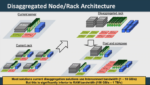
The allure of “technology resource disaggregation” – a.k.a., composable computing – doesn’t get old. It’s an ingenious yet common-sense strategy for addressing our increasingly heterogeneous HPC-AI world where no single system can cost-effectively satisfy the range of workloads needed to be kept in play, each workload having its own unique combination of system requirements that would otherwise produce, in a single system, “marooned” resources that sap budgets. Put another way, with a composable HPC infrastructure there are pools of compute, memory, and storage resources enabling the dynamic assembly of customized nodes on a per-workload basis, offering configuration of “Goldilocks” solutions.
Overcoming Bandwidth and Capacity Bottlenecks in the Exascale Era
October 21, 2021 by

[SPONSORED POST] Join us for the Advanced Memory Architectures to Overcome Bandwidth Bottlenecks for the Exascale Era of Computing webinar on November 10 at 9:00 am PT. During this webinar, leading industry experts will discuss the future of advanced memory architectures, new optical I/O solutions using silicon photonics, and the technologies and environments needed to make next-generation performance a reality.
Ayar Labs Establishes UK Subsidiary, Adds to Executive Team
June 29, 2021 by
SANTA CLARA, Calif. & LONDON — In order to address the UK and European market demand for in-package Optical I/O, Ayar Labs has established an international subsidiary with Ayar Labs UK Ltd. Optical I/O has emerged as a key technology for future high performance computing (HPC) and artificial intelligence (AI) applications. Hugo Saleh, VP of […]
Ayar Labs Demonstrates Optical Interconnect Solution on GlobalFoundries’ Silicon Photonics Manufacturing Process
December 3, 2020 by
Santa Clara, CA, Dec. 2, 2020 –Ayar Labs announced it has successfully demonstrated its patented monolithic electronic/photonic solution on GlobalFoundries’ (GF) next generation photonics technology based on its 45nm platform. This is an industry first and key milestone in providing chip-to-chip optical connectivity at scale, according to Ayar Labs, and is suited for data-hungry applications […]
The Top Five Trends Driving the Need for New HPC/AI System Architectures
November 20, 2020 by

Earlier this month Ayar Labs hosted a webinar on the topic of “Disaggregated System Architectures for Next Generation HPC and AI Workloads,” discussing the need for new architecture and the approaches that are being taken to bring new levels of power, efficiency, and composability to building the supercomputers, and eventually all computing systems of the future. Here are the top five trends that were discussed during the webinar driving the need for new HPC architectures.
Optical I/O Specialist Ayar Labs Secures $35 Million in Series B Funding
November 5, 2020 by
Santa Clara, Calif.– Nov. 5, 2020 –Ayar Labs has announced the completion of a $35M Series B financing co-led by Downing Ventures and BlueSky Capital. New investors include Applied Ventures, LLC, Castor Ventures, Downing Ventures (U.K.), and SGInnovate (Singapore), expanding Ayar Labs’ investor base with strategic ecosystem and global investors. Existing investor participation includes BlueSky […]
Paradigm Change: Reinventing HPC Architectures with In-Package Optical I/O
July 22, 2020 by

This white paper from Ayar Labs, “Paradigm Change: Reinventing HPC Architectures with In-Package Optical I/O,” discusses an important innovation: reinventing HPC architectures with in-package optical I/O. The introduction of in-package optical I/O technology helps HPC centers accelerate the slope of compute progress needed to tackle ever-growing scientific problem sizes and HPC/AI convergence.
Paradigm Change: Reinventing HPC Architectures with In-Package Optical I/O
July 20, 2020 by Leave a Comment
In this white paper, our friends over at Ayar Labs discuss an important paradigm change: reinventing HPC architectures with in-package optical I/O. The introduction of in-package optical I/O technology helps HPC centers accelerate the slope of compute progress needed to tackle ever-growing scientific problem sizes and HPC/AI convergence. Ayar Labs expects to not only see its technology extend the traditional type of architecture to put the HPC industry back on track, but also result in an inflection point that fundamentally changes the slope of the compute performance efficiency curve. The key will be enabling converged HPC/AI centers to build systems with disaggregated CPUs, GPUs, FPGAs and custom ASICs interconnected on equal footing.
Reinventing HPC Architectures with In-Package Optical I/O
July 2, 2020 by

In this sponsored post, our friends over at Ayar Labs indicate that although the industry has long recognized the potential of optical I/O as a solution for many HPC challenges, it is only in recent years that economic in-package optical solutions have become available. At last, optical I/O has emerged as the best solution to drive the next phase of Moore’s Law-like advances in post-exascale systems performance. In part this is because there have not been game-changing breakthroughs in the materials used in traditional interconnects.