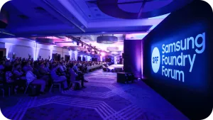
![]() At its Foundry Forum today in San Jose, Samsung Electronics spotlighted its foundry business strategy with emphasis on high performance computing (HPC), artificial intelligence (AI), 5/6G connectivity and automotive applications. A featured announcement: Samsung committed to bringing 1.4-nanometer (nm), for production in 2027.
At its Foundry Forum today in San Jose, Samsung Electronics spotlighted its foundry business strategy with emphasis on high performance computing (HPC), artificial intelligence (AI), 5/6G connectivity and automotive applications. A featured announcement: Samsung committed to bringing 1.4-nanometer (nm), for production in 2027.
That will be preceded by the introduction of 2nm process in 2025 and follows its latest 3nm process technology that is in mass production now, the company said.
“Samsung is also accelerating the development of 2.5D/3D heterogeneous integration packaging technology to provide a total system solution in foundry services,” the company said in its announcement. “Through continuous innovation, its 3D packaging X-Cube with micro-bump interconnection will be ready for mass production in 2024, and bump-less X-Cube will be available in 2026.”
Samsung also said it will enhance its gate-all-around (GAA)-based 3nm process support for HPC and mobile, while diversifying the 4nm process specialized for HPC and automotive applications.
Samsung plans to expand production for the advanced nodes by more than three times over current capacity by 2027. Including the new fab under construction in Taylor, Texas, Samsung’s foundry manufacturing lines are in five locations: Giheung, Hwaseong, and Pyeongtaek in Korea; and Austin and Taylor in Texas.
Samsung also detailed its ‘Shell-First’ strategy for capacity investment, building cleanrooms first irrespective of market conditions. With cleanrooms readily available, fab equipment can be installed later and set up flexibly as needed in line with future demand, the company said. Through the new investment strategy, Samsung will be able to better respond to customers’ demands.
Also unveiled were investment plans in a Shell-First manufacturing line in Taylor following the first line announced last year, as well as potential expansion of Samsung’s global semiconductor production network.
Samsung said it will hold its ‘SAFE Forum’ (Samsung Advanced Foundry Ecosystem) on October 4 showing new foundry technologies and strategies with ecosystem partners encompassing areas such as Electronic Design Automation (EDA), IP, Outsourced Semiconductor Assembly and Test (OSAT), Design Solution Partner (DSP) and the cloud.
In addition to 70 partner presentations, Samsung will introduce the possibility of applying Samsung’s processes, such as design technology co-optimization for GAA and 2.5D/3DIC.
As of 2022, Samsung said it provides more than 4,000 IPs with 56 partners and is also cooperating with nine and 22 partners in the design solution and EDA, respectively. It also offers cloud services with nine partners and packaging services with 10 partners.
The Samsung Foundry Forum will be sequentially held in Europe (Munich) on the 7th, Tokyo on the 18th, and Seoul on the 20th.