And it all gets sealed with an engagement to ORNL
 Today NVIDIA’s CEO Jen-Hsun Huang delivered the keynote address at the GPU Technology Conference in San Jose, and gave a big fat kiss to folks looking to get extra performance for their computations out of NVIDIA’s GPUs. Huang announced Fermi, NVIDIA’s third generation GPU architecture, which NVIDIA is pitching as “the soul of a supercomputer in a GPU.” There is a lot that is new here, so let’s start at the beginning and break it down.
2x the cores
NVIDIA’s goal with Fermi is to bring more users and more applications to GPU computing, and many of the changes they’ve made this time are aimed at enlarging the domains in which GPUs make sense. The new design has 512 cores, and NVIDIA has engineered a design with 8x the double precision performance of the last generation. This is more than double the core count in about 12 months, leading us to get pretty excited about the idea of >1024 threads by 2011.
Fermi’s double precision performance now runs at about 50% of the single precision performance (makes sense, it takes 2 32-bit lines to move the data around), a ratio that is 5 times better than the last generation GPU could manage. The accuracy of double precision computations has also been improved with support for the new IEEE 754-2008 floating-point standard, and a fused multiply-add instruction. Fermi can issue 512 FMAs per clock in single precision, or 256 FMAs per clock in double precision mode.
Real cache, more RAM, and ECC (finally)
Also targeted at winning over new users is the introduction of a cached memory hierarchy, the first NVIDIA GPU to do so. The new design features a dedicated 64KB L1 cache per Streaming Multiprocessor (GPU cores are organized hierarchically into “Streaming Multiprocessors,” or SMs; 32 cores form an SM, and there are 16 SMs on a board), and a 768KB L2 cache shared among all SMs. NVIDIA calls this the “Parallel DataCache Hierarchy,” and Sumit Gupta, senior manager in the Tesla GPU Computing group, says that this feature is very important not only to sparse matrix and physics calculations (for gaming), but also for traditional graphics applications like ray tracing. Application engineers should now see a much more familiar programming environment when porting code from CPUs.
Speaking of memory, there’s more of it — a lot more. The previous GT200 architecture had a 4GB physical limit on the amount of memory that could be connected to the cards. With Fermi NVIDIA’s engineers have moved to 64-bit memory addressing, and the architecture will now theoretically support up to 1 TB of RAM on a single card. It’s pretty unlikely that there will be a standard SKU with that much memory, but certainly cards with 6 GB or more of memory should be economically viable. Fermi also supports the faster GDDR5 memory interface (the GT200 generation supported GDDR3 memory) and ECC, addressing a big concern that users had for the reliability of data. According to Gupta this is the first GPU to support ECC for the RAM itself — ATI’s GPUs use GDDR5 and offer data link protection for errors that could occur during data transfer, but that is part of the DDR5 standard (and Fermi has this as well). All the major internal memories are ECC protected, including the register file and both the L1 and L2 caches. GDDR5 is theoretically about twice the bandwidth of GDDR3, but the actual speeds and feeds will vary with the specific products built on the Fermi architecture. I would also expect GDDR5 to add a premium to the price, at least at first.
Hardware thread scheduling and concurrent kernel execution
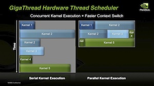
 A big step forward in improving the application sweet spot for GPUs is the change in the way threads are scheduled. NVIDIA’s GigaThread Hardware Thread Scheduler (HTS) handles all of the task scheduling for developers who are now free to just throw tasks at the GPU without having to worry (as much) about packing the tasks together to efficiently manage the resource. The old architecture executed individual tasks one at a time (see image to the right) and had a relatively slow context switch, so developers had to be sure they sent large pieces of work to the GPU in order to get anything like good performance. The new HTS supports concurrent kernel execution and context switching that’s about an order of magnitude faster than before, so now much smaller units of work can be sent to the GPU. If you think of work kept on the CPU as the “serial fraction,” then these two changes should help move the Amdahl performance limit for GPU-accelerated applications further to the right.
If you are worried about keeping the CUDA kernels busy while you are doing all this concurrent kernel execution (and you should be worried about that), then you’ll be happy about the new twin DMA engines in Fermi. With the single DMA of the GT200, developers could overlap communication and computation in one direction, for example writing a result back to the CPU while they computed a new result. But with dual DMA, applications can write to and read from the CPU while computing, allowing for full overlap of communications and computation, and again helping to expand the set of applications that can potentially benefit from a GPU assist.
NVIDIA adds IDE, C++, and (thank goodness) print debugging
But what about the software that makes it all work? NVIDIA announced earlier this week that a new FORTRAN compiler for CUDA had entered beta, a big deal for the scientific computing community. With Fermi NVIDIA is adding full support for C++ to the already existing support for C, including the hardware needed to support exception handling and virtual functions. Fermi will also support system calls for the first time on the GPU, so that file streaming will no longer have to be mediated by the CPU and printf debugging is at long last possible (yeah, I know, it’s not exactly modern, but we all still do it). When you step back and look at it, NVIDIA has done a lot to make their general purpose GPU pretty general purpose. With support for C, FORTRAN, C++, Python, Java, OpenCL, OpenGL, DirectCompute, and DirectX 11 there is something for just about everyone here.
NVIDIA is also announcing a new Integrated Development Environment that will be available this week, called Nexus. Nexus integrates into MS Visual Studio 2008 and, according to Gupta, has been designed to speed up CPU+GPU computing. Two versions of Nexus will be available: Nexus Standard and Nexus Professional. Nexus Standard is available at no cost to developers, and includes basic source debugging and profiling functionality that matches existing functionality with PerfHUD. Nexus Professional includes advanced debugging features, full system event tracing, and premium support; it will retail for $349.
A vote of confidence: plans for a big super at ORNL
Today’s announcement by Huang focuses on the architecture, not the specific products. Those won’t start showing up until “sometime next year” according to Gupta. While the company declined to be more specific with us on release dates, there are at least some folks out there that know a little bit more about the schedule and are pretty excited about the technology. Today we also learned that Oak Ridge National Laboratory is planning to build a supercomputer based on Fermi products. From a statement released by the company during the announcement
“This would be the first co-processing architecture that Oak Ridge has deployed for open science, and we are extremely excited about the opportunities it creates to solve huge scientific challenges,” Nichols said. “With the help of NVIDIA technology, Oak Ridge proposes to create a computing platform that will deliver exascale computing within ten years.”
That’s a pretty awesome announcement for a design that isn’t even a product yet.


[…] NVIDIA’s next generation GPU architecture has a lot for HPC to love | insideHPC.com. Related News & Resources nVidia GT300 unveiled: 512 cores, up to 6GB GDDR5 nVidia […]