By Rik Myslewski in San Francisco • Get more from this author
Analysis There are two reasons why Intel is switching to a new process architecture: it can, and it must.
 The most striking aspect of Intel’s announcement of its new Tri-Gate process isn’t the architecture itself, nor is it the eye-popping promises of pumped-up performance and dialed-down power. And it certainly isn’t the Chipzillian marketeers’ risible emphasis on “3-D”.
No, it’s that Intel has not only the know-how and ready cash, but also the never-surrender cajones to pull off such a breakthrough. The world’s number-one microprocessor designer is not content to merely dominate some sectors of the market for silicon brains, it wants its parts to be in every thinking device, from the lowliest embedded systems to the brainiest HPC clusters.
And Intel is willing to invest – bet? – big to make that happen.
The move to a 22nm Tri-Gate process architecture is an important step for Intel’s entire microprocessor line, but it’s especially critical for the company’s desire to enter the low-power world of tablets and smartphones – and whatever consumer-level world-changers might appear next.
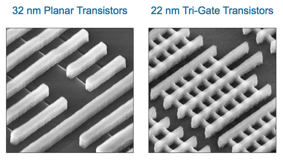
But although Tri-Gate is undeniably a breakthrough – more on the deep-tech details in a moment – it was not an unexpected one. The basic idea behind what Intel calls Tri-Gate is amalgamated into a concept that the rest of the known universe calls FinFET – cute geek-speak for a vertical “fin” of silicon poking up into a field-effect transistor’s gate.
A fin in a FET – get it? There are a number of FinFET-ish architectures under study in labs around the world. Intel calls theirs Tri-Gate, due to the fact that the fin has a left, right, and top surface upon which charge can flow through the gate.
FinFET-based process architectures are far from new. Intel has been futzing around with the concept since 2002, and the Taiwanese chip-baking giant TSMC demonstrated a 25nm FinFET design it dubbed “Omega” at about the same time.
What Intel has now done, however, is not merely demo another FinFET concept, but to throw the full weight of its manufacturing prowess and financial clout behind FinFET Tri-Gate, and move its entire microprocessor line to the new process.
Intel’s breakthrough isn’t conceptual and lab-based, it’s real and market-based.
And it’s very, very expensive. Intel is spending $8bn to upgrade four fabs in Oregon, Arizon, and Israel to 22nm Tri-Gate, and to create a fifth one, also in Oregon, from scratch. At the same time, by the way, Intel is also investing a good chunk of its $10.2bn 2011 capex budget on the development fab for its upcoming 14nm process, and bulding that fab bigger than originally planned.
Eight billion dollars for 22nm Tri-Gate fabs is not chump change – especially to a company that recently bought McAfee for $7.7bn and Infineon for $1.4bn, and that spent over $7bn since early 2009 on other fab upgrades.
Oh and let’s not forget the little $1bn annoyance that was the Cougar Point chipset flaw this winter.
But Intel has the resources it needs to move to 22nm Tri-Gate. After all, acquisitions, capex, and “oops” are not the only ways that the company is doling out cash these days. The company also spent $4bn to repurchase 189 million shares of common stock in its most recent quarter – a quarter during which it also paid just under $1bn in dividends to stockholders. (Are you listening, Steve Jobs?)
Not that Intel has a cash horde equivalent to Apple’s $66bn: its cash and cash equivalents, short-term investments, and trading assets total just under $12bn. But compare that with its closest microprocesser rival, the fabless AMD, which has just $1.75bn in the bank. Intel’s market capitalization is $127bn; AMD’s is $6bn.
Intel’s other main rival, of course – and one that’s growing in importance – is also fabless and also goes by a TLA: ARM. If Intel’s engineering chops and deep pockets are the proof of the “because it can” reasoning behind its move to Tri-Gate, ARM – and, to a lesser extent, AMD – is the driving force behind “because it must”.
Let’s back up a few years to 2007, the year in which Intel introduced its most recent Really Big Thing™ in process technology. That’s the year when the company replaced the traditional silicon dioxide gate dielectric in its microprocessors’ transistors with a high-k metal gate, which increased gate capacitance, thus improving performance while significantly reducing current leakage.
The high-k metal gate helped make it possible to shrink that generation’s process technology to 45nm. And we’re all familiar with the process-shrinking mantra: smaller processes mean lower power, faster performance, less heat, Moore’s Law lives to fight another day, and blah, blah, blah.
The difference, however, between 2007 and today was that four years ago Intel was riding high with nary a serious threat in sight (sorry, AMD fans). The company’s move to the 45nm “Penryn” line was arguably prompted mostly by a desire to induce upgrades from users of the previous generation of 65nm “Conroe” processors, and to sell data center folks on the cost savings of lower-power parts.
That was then. Things have changed.
Fast forward to 2011: Chipzilla under threat
The situation today is quite different. While Intel still squats in more server sockets than its AMD competition, down in the consumer space its hegemony is in question. The market-watchers at IDC, for example, predict that ARM will suck up 13 per cent of the PC marketplace by 2015, due mostly to Microsoft porting Windows 8 to ARM in 2012 or 2013.
AMD is a resurgent threat, as well, with its new Fusion line of CPU/GPU mashups that AMD insists upon calling APUs – accelerated processing units. Intel’s vastly greater marketing and distribution resources will surely make it difficult for the “li’l microprocessor designer who could” to tear significant chunks of market share away from Chipzilla, but don’t think they won’t try – and, with ATI graphics chops on their APU silicon along with new Bobcat and Bulldozer cores, don’t think they won’t succeed to an Intel-annoying degree.
Down in the exploding tablet and smartphone space, Intel is, well … to call their current position “suboptimal” would be kind. The company’s pioneering low-power efforts – “Menlow” and “Moorestown” – were essentially failures, and the jury is still out on its most recent effort in this space, “Medfield“.
ARM – with its IP being embodied in silicon by chip-bakers such as Samsung, Qualcomm, Nvidia, TI, and others – owns the tablet and smartphone market.
But what must be even more troubling for Intel is that ARM is moving up into the PC market – as evidenced by IDC’s predictions noted above, and soon to be boosted by the consumer-level, PC-capable ARM Cortex-A15 design, scheduled to appear next year in chips from TI, Nvidia, and others.
Just to put an additional frisson of fear into Intel’s corner offices came a rumor this Friday that Apple – Intel’s BFF since the first Chipzillian Macs shipped in 2006 – is mulling a switch to ARM for its hella-popular laptops (at minimum) in the next two or three years.
Intel is finding itself threatened at the growing low-power end of the consumer spectrum in a way that it has never been before. (It’s also facing challenges in the server space from such new developements as microservers and massively multicore processors from outfits like Tilera, but those threats are not as immediate.)
So when a company is threatened, what does it do? It falls back on its strengths. And what are Intel’s strengths? Engineering smarts and cash. And it took both to bring the Tri-Gate design and manufacturing process into fruition.
You might also argue, of course, that another of Intel’s strengths is the gargantuan installed base of Intel-architecture apps littering God’s green earth – and you’d have a good argument, if you were talking about PCs. Tablets and smartphones, not so much – which is, of course, why Intel is busily porting Android’s tablet-centric version 3.0 to IA.
But exactly how good is 22nm Tri-Gate, and will it be fast enough and low-power enough to move Intel into the range it must comfortably inhabit if it’s going to compete with ARM?
The simple answer to that question is: “Dunno.” After all, it will be a while before we get our hands on 22nm Tri-Gate microprocessors. All we have so far are presentations and promises. However, if what Intel revealed on Wednesday is even close to the truth, there a chance that the first procs to be built using the process, which will be code-named “Ivy Bridge”, might be worthy competitors.
With the help of Intel senior fellow Mark Bohr, who provided a technical overview of Tri-Gate at the rollout – plus enduring one of the more embarrassing marketing-video starring roles we’ve seen in some time – let’s take a bit of a deep dive into the transistor tech that Tri-Gate embodies.
Deep – really deep – inside Tri-Gate
As we mentioned earlier, Tri-Gate is a variation of the FinFET concept, in which instead of lying below the gate as in a traditional planar transistor design, the charge-carrying silicon pokes up into the gate itself.
 In a planar design, gates were lain across a flat silicon substrate – not 3-D enough for marketeers, however.
This non-planar construction, by the way, is why you’ll hear Intel marketeers exalting the Tri-Gate design as “3-D”. Well, yeah, that’s not entirely untrue, but the gate-wrapped fin is hardly 3-D enough to warrant such buzz-lines as this one from the Wednesday presentation: “Transistors have now entered the third dimension! – and, yes, that’s Intel’s italics and Intel’s exclamation point.
In any case, you might reasonably ask: “So the fin sticks up in the gate? So %$#@!ing what?” Bohr’s answer to that perfectly reasonable question is equally reasonable: “The key advantage of this structure – and it comes from the fact that the gate wraps around this fin – [is that] it provides fully depleted operation of the transistor.”
Bohr’s answer, of course, is only reasonable if you know why a fully depleted transitor is a good thing – which takes a bit of background to explain.
When a traditional microprocessor transistor is in the “on” state, current flows from source to drain through what’s called the transistor’s “inversion layer”, which interacts in Intel’s designs with the transistor’s high-k metal oxide interface with the gate. That’s all well and good.
However, when the transistor is in the “off” state, some charge can still trickle through the silicon substrate. When it does, the transistor is regarded as not being fully depleted. That’s bad.
When voltage hangs around like this, it degrades what chip boffins call the “sub-threshold slope” of the transistor – which Bohr defined as “essentially the transistor turn-off characteristics,” or which we can think of as how “off” the off state actually is.
When the transistor’s off state is fully depleted, it helps minimize power usage. Also, a fully depleted transistor can have a lower threshold voltage – meaning that the voltage needed to switch it from off to on can be lower, again saving power.
When you operate at a lower threshold voltage,” Bohr explains, “you have improved performance. Or you can operate at lower voltage, and if you operate at lower voltage, there’s a significant active-power saving – and that’s really probably the most important advantage of Tri-Gate.”
So, a fully depleted transistor both leaks less power and requires less power. All good.
Planar processors are hell to make fully depleted. In their traditional state, there’s a lot of room in the silicon substrate to house errant voltages. You can, however, add an oxide insulator below the source and the drain to create what’s called a partially depleted silicon-on-insulator (PDSOI) design.
You can go all the way to fully depleted (FDSOI) without going FinFET by depositing an extremely thin SOI layer on top of the oxide – but reaching full depletion this way is quite expensive. According to Bohr, baking a chip this way adds at least 10 per cent to the total wafer cost.
Tri-Gate, by comparison, is cheap. “Another nice thing about the Tri-Gate devices,” Bohr says, “is that they’re not that expensive to add. Compared to a planar version of 22 nanometers, Tri-Gate transistors add only about 2 to 3 per cent cost to the finished wafer.”
The Tri-Gate way of reaching full depletion is to stick that silicon fin up into the gate, have the inversion layer on both sides and the top of the fin, with the high-k metal oxide of the gate snug against the inversion layer. Presto – no room for nasty voltages to accumulate, plus the larger wrap-around inversion layer and metal-oxide interface allow for more current, and thus better performance. Bonus!
Another nifty Tri-Gate trick is that you can have multiple fins in the same transistor: more fins, more current, better performance. Or, as Bohr puts it succinctly: “You can gang together these fins to create larger transistors with higher drive currents.”
This “How many fins do you want?” capability will help Tri-Gate to populate throughout Intel’s product line, from low-power single-fin transistors to multi-fin structures that will find their way into Xeons – and even into Itaniums, when that benighted chip reaches its Kittson incarnation, two generations from today’s 9300 series.
ll well and good, but so what?
All this techy-techy yumminess is good geeky fun, but what does it all add up to? How much improvement are we to expect out of the Tri-Gate process upgrade?
Quite a bit, if Intel – and Bohr – are to be believed.
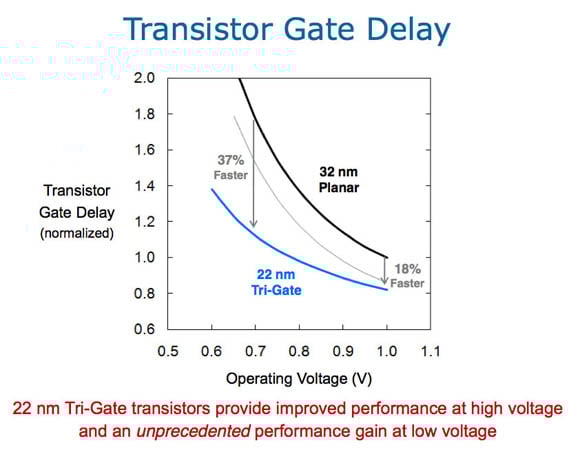
The 22nm Tri-Gate transistors will, according to Bohr, provide much-improved performance at low voltages. The examples he provided were based on gate delay as one variable, which in a transistor increases as power decreases. “When you operate [any transistor] at a lower votage, it tends to slow down. Think of gate delay as the inverse of frequency: higher gate delay means slower frequency,” he said.
 Much faster at far less power – what’s not to like?
“In this example,” he explained while displaying the slide above, “at 0.7 volts they’re about 37 per cent faster than today’s 32nm planar transistors.” And to cut naysayers off at the pass, he added: “And I want to emphasize that this 32-nanometer curve – that’s not just some dummy straw man, those are the fastest planar transistors in the industry today,” adding with a trace of pride: “That’s Intel’s technology.”
What happens, though, when you operate a 32nm transistor and a 22nm Tri-Gate transistor at the same gate delay? You’d assume lower power consumption for the Tri-Gate, right? But how much lower? A glance at Bohr’s Gate Delay slide shows that when the 32nm planar and 22nm Tri-Gate transistors are both operating at a gate delay normalized to 1.0, the power savings are considerable.
If you operate them at the same gate delay, the same frequency,” he said, refering to the two transistor types, “to get the same performance from [Tri-Gate] as planar, you can do so at about two-tenths of a volt lower voltage – in other words, at 0.8 volts instead of 1 volt. That voltage reduction, combined with the capacitance reduction that comes from a smaller transistor, provides more than a 50 per cent active-power reduction.”
Then, in Wednesday’s understatement, Bohr concluded: “And that’s very important.”
To sum up: at the same voltage, 37 per cent faster performance. At the same clock frequency – inferred from gate delay – a 50 per cent reduction in power.
Not too shabby, if true. Remember, though, that these aren’t benchmark figures derived by independent testing, they’re numbers taken from slides presented by an Intel senior fellow at the rollout of his baby.
Your mileage may vary.
Still, Tri-Gate may allow Intel to both maintain IA’s lead in the server space while lowering cooling and power costs, and find it a new home in the low-power consumer space.
If, however, Tri-Gate doesn’t perform as promised, Intel may have blown its last chance of entering the lucrative, growing, and ultimately consumer-consuming low-power mobile market.
Or, for that matter, Intel could license the ARM architecture and start buiding its own ARM variants in its own fabs, using its 22nm Tri-Gate process. That’s unlikely, but stranger things have happened – such as Intel, once the seemingly unchallengeable PC overlord, being threatened in the consumer-PC market by Windows-running, 40-bit addressing, multicore ARM Cortex-A15 chips. ®
This article originally appeared in The Register.


[…] http://insidehpc.com/2011/05/09/intels-tri-gate-gamble-its-now-or-never/ […]