By Rik Myslewski in San Francisco • Get more from this author
 AMD’s new graphics architecture isn’t merely about painting prettier pictures. It’s about changing the way computers compute.
As first revealed last month at AMD’s Fusion Developer Summit, the chip designer has gone out of its way to ensure that its future APUs – accelerated processing units, which is what the company calls it CPU/GPU mashups – don’t merely relegate the CPU and GPU to being neighbors sharing the same slice of silicon. It seeks to make the CPU and the GPU full partners in whatever a computer’s operating system and apps can throw at them.
The idea of this workload sharing, sometimes called general-purpose GPU computing (GPGPU), first gained public awareness in 2004, when a group of seven computer-science researchers from California’s Stanford University presented a paper at that year’s SIGGRAPH conference on a programming environment called Brook for GPUs. That research was the seed of what has became known as GPU compute, general-purpose computing on GPUs, or simply GPGPU.
That effort to leverage the massive parallelism of GPUs to offload appropriate compute tasks from CPUs really began to take off in 2007, according to AMD graphics CTO Eric Demers, accelerating in 2009 as DirectCompute and OpenCL began to win adherents.
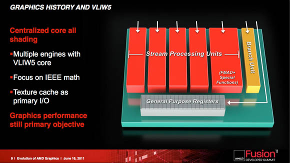
Still, the ATI – now AMD – GPUs of the time were based on a relatively straightforward VLIW (very long instruction word) architecture that was designed and tuned for graphics. GPGPU usage was secondary. “This architecture – when we start using it for generalized compute – works okay,” Demers said at the Fusion Developer Summit, “but it leverages the graphics.”
Ah, the simple days of very-long-instruction-word graphics engines (click to enlarge)
In the last 12 to 18 months, however, the importance of a GPU being able to work closely with a CPU has become more important in AMD’s designs. Graphics performance is still the central goal, but there are other goals as well.”We are making significant optimizations for compute,” Demers says. “We are looking at things differently.”
Demers offers AMD’s January 2011 HK-2207 demo – which, incidentally, was ridiculed by an Nvidia exec – as an example of this new thinking. “This demo uses GPU to do all the particle physics,” he says. “It uses deferred lighting with G-Buffers, it does post-processing as a compute operation – it does very complex operations. And what is compute and what is graphics is blurred.”
Graphics meet compute. Compute meets graphics
AMD has revealed a roadmap of its effort to continue the blurring of the line between graphics and compute, dubbed the Fusion System Architecture (FSA). This ambitious wish list seeks to combine the CPU and GPU into a single computing team by simplifying the programming model, unifying the memory being accessed by CPU and GPU, lowering the latency of task dispatching between CPUs and GPUs, and other enhancements.
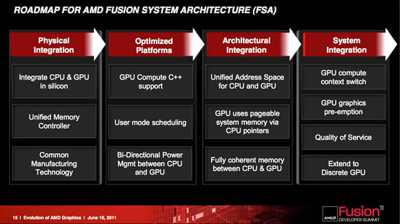 The first column of AMD’s FSA roadmap is essentially complete. Work on the others is underway (click to enlarge)
To accomplish all the goals of the FSA, Demers says, requires rethinking the GPU core. And so over the past three years AMD engineers have being doing just that, with the result being the company’s next-generation graphics architecture, dubbed Graphics Core Next (which, of course, has its own TLA: GCN. The GCN is a fundamental piece-by-piece rethinking of the former ATI/AMD architectures.
The heterogeneous future
GNC’s goal is twofold: simplify the programming model and make the GPU core more capable of participating in what AMD, ARM, Microsoft and others call “heterogenous computing” – that is, distributing work among CPU, GPU, and more-specialized cores, which each element contributing what it does best.
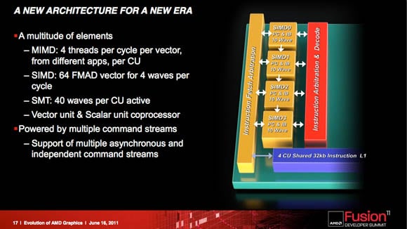
The major change in the GCN’s shader array is that it includes what AMD calls the compute unit (CU), and what Demers calls the “cellular basis” of the design. A CU takes over the chores of the previous architecture’s VLIW-based SIMD (single-instruction-stream, multiple-data-stream) elements.
VLIW is gone. The GCN’s CUs are fundamentally vector cores containing multiple SIMD structures, programmed in a per-lane basis. Four groups of wavefronts are run in each CU core per cycle. “It’s a vector core where each lane is programmed independently, and there’s a single stream coming in and broadcast all over those things,” Demers says. “You program it in a scalar way, and it operates in a vector mode.”
Simply put, a CU might be considered to be a smart VLIW/SIMD structure. In the VLIW world, you’d have to rely on the compiler to load the core correctly and efficiently. If something changes in the instruction stream, the VLIW is too dumb to modify its workload, and pipes might remain unfilled with data, wasting cycles.
As you might guess, that makes VLIW perfectly fine for graphics, where predictability is high, but crappy for compute, where dependencies can and do change at a moment’s notice – even if that “moment” is a billionth of a second. Although the CU must work wavefront by wavefront – it’s not an out-of-order mind-reader – it can move workloads around radically more nimbly than VLIW.
Core reasoning
This versatility is the – pardon the pun – core reason for the GCN: AMD is planning for a heterogeneous world, in which GPUs are increasingly equal compute partners with CPUs.
The CUs can work in virtual space, Demers says, and they’ll support the x86 64-bit virtual address space – more on that later. Also, the CUs are supported by a much larger L1 data cache than was in the previous architecture. The cache also has what Demers calls “a significant amount of bandwidth,” and is supported by its own control system.
Previous AMD GPU architectures have had what the company has called “hidden fixed-function with hidden state”. As examples of such fixed functions, Demers identifies “program counter advancements, and things such as that – limited functionality.”
Help with the housekeeping
The GCN moves beyond hidden fixed functions with the addition of a fully observable scalar processor, which frees the CUs from simple tasks – quick math functions, for example, and housekeeping. “It’s a processor in its own right,” says Demers, and it’s responsible for such common code as branching code and common pointers. A vector unit could also handle such common-code chores, but as Demers explains: “The scalar coprocessor helps it out, and offloads those capabilities.”
Observability of the CUs and the scalar processor, and support for the x86 virtual space – along with the fact that, Demers says, “you can load the PC from memory or from a register and do all kinds of math” – opens up such C++ features as virtual functions, recursions, and x86 dynamic linked libraries. “All of these become a native thing that this guy can support,” he says.
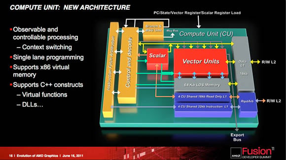 Shrinking processes enable more stuff to be stuffed on a chip – so let’s add a scalar processor (click to enlarge)
The processing capability boosted by a host of compute units is all well and good, but only if they can be fed the right data to munch on at the right time. To this end, the GCN architecture allows for multiple command streams from multiple applications, each with different priorities and the ability to reserve CUs for themselves.
As an example of this capability, Demers suggests the interaction of your operating system’s user interface and an app. “You can have your GUI running at one priority level, and you can set that high, and you can guarantee some amount of compute units always available for it. But then your big background applications for transcode can be running at a lower priority,” he says, and you will still have a great quality of service [QoS] – there’s no more skipping mouse when you do a big job, because the big job is running in a separate queue.”
Thanks for the (shared) memory
To feed all those command streams, Demers says, a new memory system is needed. In previous AMD GPU architectures, the memory system was a read-only cache; in the new architecture, it’s read-write. “It’s a generalized cache just like we have in CPUs,” he says.
Total bandwidth between the CUs and the caches is, of course, dependent upon the number of CUs and the clock speed. Assuming a clock of around one gigahertz, “If you think of a CU as the equivalent of a SIMD – which isn’t the case, but today we ship with 24 of these – 24 CUs would be one and a half terabytes of bandwidth to their L1 caches,” Demers says. “Pretty good numbers.”
Don’t expect AMD to stick to 24-CU implementations, however. Demers talked of future designs with over a hundred CUs – and it’s not tough to do the math to figure out what the total cache bandwidth would be in such chips: 100 CUs would top 6 terabytes of total bandwidth.
To add more memory-system versatility, there’s a full interconnect between the L2 and L2 caches. “The L2s are more physically based. They match your memory,” Demers explained. “They’re also where all the coherency happens – and that’s what I mean by the physical binding of the L2s.”
The L1s get their data from their associated L2s, but the L2s – since they’re the soul of coherency – will communicate with one another. The GCN also envisions conherency being handled between both CPU and GPU at the L2 level. “I’m talking probe traffic,” Demers says, “I’m talking all the usual stuff you’ve come to expect on coherency.”
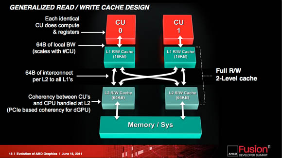 GPU CUs and CPU cores will find coherency at the L2 level. Discrete GPUs can join over PCIe (click to enlarge)
With all the CUs having access to all the data that’s in the L2 farm, time-consuming trips back and forth to and from far-off system memory would be minimized, pruning latency. Discrete GPUs will also join in the coherency mix, with all traffic being tunneled over PCIe. “Discrete GPUs and Fusion APUs will all use the same core technology,” Demers explains.
x86 spoken here
x86 support, he says, means that “our GPUs have to have address-translation caches. Basically, they take virtual addresses and they translate that into physical addresses.” Address-translation caches already exist in AMD GPUs, but in the new architecture, they’ll be talking in x86 language.
On the CPU side, “an OS-visible IOMMU [input/output memory-management unit] – just like the CPU has an MMU, which handles which handles physical to virtual translation on the CPU – needs to exist,” Demers says.
With an IOMMU – which will be part of both AMD’s discrete CPUs and APUs – the chips will be able to support address-translation requests. Demers also notes that should their be a page fault, “the GPU will be happy with that – well, not necessarily happy, but it will survive that. It will wait until that page is brought in by the operating system and made local, then – bang! – it’ll keep on running.”
The x86 address space will provide “all the goodness” that comes from a virtual address space, and will be available for the GPU in the new architecture, Demers said, specifically citing over-subscription. “Our plan is that eventually all these devices – whether CPUs or GPUs – are in the same unified 64-bit address space.”
As might be assumed due to Demers’ page-fault example, OS support will be required for IOMMUs, just like it is on MMUs, so AMD is now working with operating-system designers. Although he didn’t specifically say which ones, Microsoft’s presence at AMD’s event might well be counted as a major hint.
All these features will stretch across AMD’s graphics-capable product line. “I’m not talking about an APU, I’m not talking about a GPU, I’m talking about an IP of a core that’s going to be used in all our products going forward,” Demers says. “Over the next few years we’re going to be bringing you all of this throughout all of our products that have GPU cores.”
Meat and potatoes
Despite spending a raft of development time on this fundamentally different GPU architecture, AMD also spent some time digging into such meat-and-potatoes graphics necessities as good ol’ 3D performance.
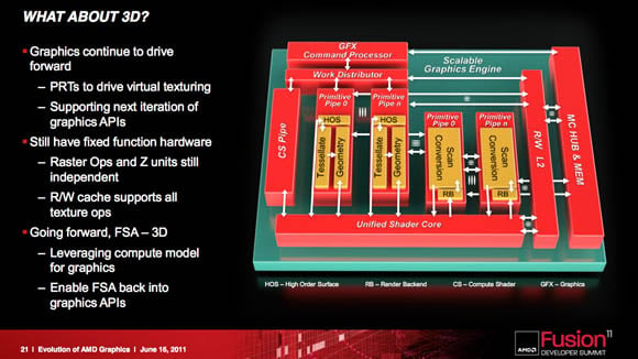 Heterogeneity is all well and good, but AMD has some 3D improvement in mind, as well (click to enlarge)
“I did say that 3D and compute are starting to merge – and in my mind they already have,” Demers says. “Somebody recently asked me about APIs – well, we’re full of ideas for graphics. And we still love APIs and we think that developers will continue to use APIs.”
He suggests that some developers will want to “go directly to compute,” but he said that AMD would continue to work with partners such as Khronos – the OpenCL caretaker – and DX11-provider Microsoft to expose to devs more features that AMD provides in its hardware.
As an example of something that the new architecture will support, Demers offers partially resident textures (PRTs), which he defined as the ability to “tell an application: ‘Look, create textures of any size you want, and then bring in the parts that you need when you want them’.”
2013 and beyond
All this new stuff doesn’t mean that all the old stuff has been jettisoned. Fixed-function elements such as Raster Ops and Z units, for example, are still there with their own caches. “We don’t want to get rid of any things that are good in our core,” Demers says. “We’re going to continue to drive [fixed-function features] forward and continue to put more of those units [on chip] as cost and process allow us.
The read/write cache in the GCN will also be available as a texture cache. “Larger caches, higher throughputs – those are going to benefit texturing as well,” Demers says. In addition, true virtual memory will enable such niftiness as being able to pre-compute massive scenes and load portions only as needed, smoothing performance.
“I really am excited about Fusion System Architecture (FSA) and 3D merging,” Demers says – excitably, as one might imagine. “Compute, and graphics APIs, and hybrids of all those things – it’s really cool.”
Unfortunately, you’ll have to wait a while to experience that coolness. AMD’s Bulldozer-based APU, Trinity, which was demoed on the same Fusion Summit stage two days before Demers’ presentation, will be VLIW-based when it appears next year. Best-guesstimates put GCN-based APUs somewhere in the 2013 time frame.
With the introduction of FSA and the GCN – oh, and let’s not forget the Bulldozer and Bobcat CPU cores – AMD is betting the farm that the future will belong to heterogeneous computing, where tasks are given to various and sundry cores according to the ability, and distributed from apps according to their need.
For AMD’s sake, let’s hope that if they have seen the future, and that their implementation works better than did the terrestrial analog of that to/from equation. ®
This article originally appeared in The Register.



[…] Deep Inside AMD’s Master Plan to Topple Intel, and NVIDIA. […]