[SPONSORED GUEST ARTICLE] As the HPC-AI juggernaut races ahead with larger and more complex models built for more demanding AI workloads, the massive compute engines required to train and run them contain a critical flaw that will, ultimately, hamstring HPC-AI’s insatiable appetite for more powerful systems.
It’s the problem of traditional copper-based electrical interconnects that move data from storage to memory to compute, within and among chips and servers. This creates I/O performance bottlenecks as well as high heat. In HPC, this is a problem of long-standing. The combination of HPC and AI only exacerbates it.
To be sure, the HPC-AI community isn’t waiting around for a solution, it’s moving forward with larger models using increasing volumes of data requiring bigger systems, all the while adopting more elaborate interconnect bottleneck workarounds. This means increasingly imbalanced and hotter server clusters and data centers that are falling short of the performance advancements and energy efficiency needed for advanced HPC-AI.
This is why developments in photonics-based interconnects are so intriguing, offering the promise of increasing bandwidth by up to 1000x at 10 percent of the power consumption of electrical I/O. As participants in a session at the recent SC23 supercomputing conference in Denver said, it’s about enabling cooler, composable systems that don’t have “glow-in-the-dark GPUs” and move data “without burning a hole in the side of our board.”
That SC23 session, “Scalable and Adaptable Architectures for AI/HPC Advancement,” examined predictive analytics, physics, modeling and new use cases for generative AI driving model size increases of 10x every 18 months and how to deal with the resulting I/O bandwidth challenges.
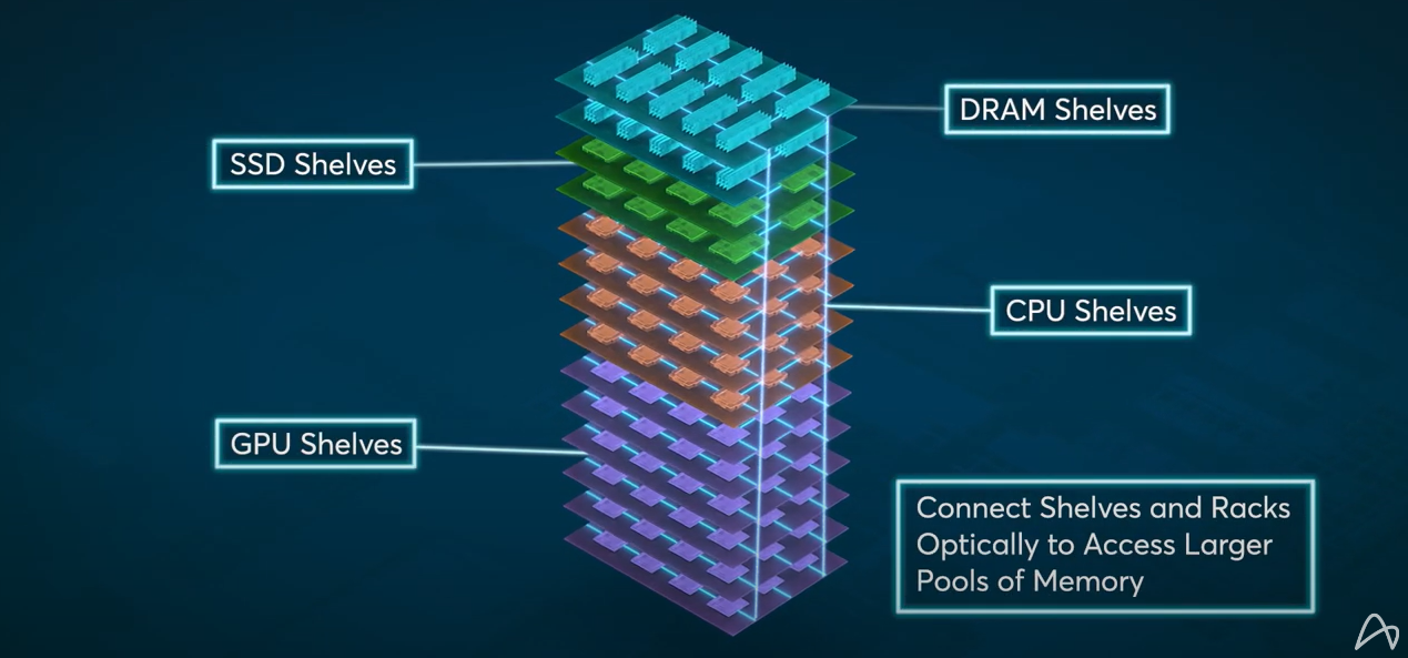
Disaggregated computing (credit: Ayar Labs)
The session’s participants included senior managers from silicon photonics startup Ayar Labs, from Columbia University, Lawrence Berkeley National Laboratory, the University of Bristol, Intel, NVIDIA and Xscape Photonics.
Columbia’s Karen Bergman, the Charles Batchelor Professor of Electrical Engineering and Faculty Director of the Columbia Nano Initiative, described the scale of the interconnect challenge.
“AI model sizes have increased by roughly an order of magnitude a year over the last five or six years, and there is no sign of that slowing down,” she said. “In fact, there’s an acceleration of that, we’re up to trillions of parameters in these very large training models. What’s important here is they exceed the memory capacity that we have within the socket, within the node.”
This is why IT strategists believe there’s much potential with composable, or disaggregated, computing, in which “pools” of compute resources are assembled for workloads on a customized, case-by-case basis. According to John Shalf, Department Head for Computer Science Lawrence Berkeley Lab and a member of the SC23 panel, composable computing has been increasingly adopted in data centers and by hyperscalers.
Composability stands in contrast with the conventional way systems are deployed. As Shalf described it, “You basically start with a server and you pack into it everything that you think you might need, the worst-case memory capacity, maybe some local NVRAM, whatever accelerators you want…, and then you replicate and repeat as you scale out your system until you run out of funding.” The result: systems are commonly over-provisioned, wasting money.
While composability is an attractive alternative, electrical interconnects pose I/O performance problems for data- and compute-intensive HPC-AI workloads because of the physical separation – the distance between – disaggregated compute and storage resources.
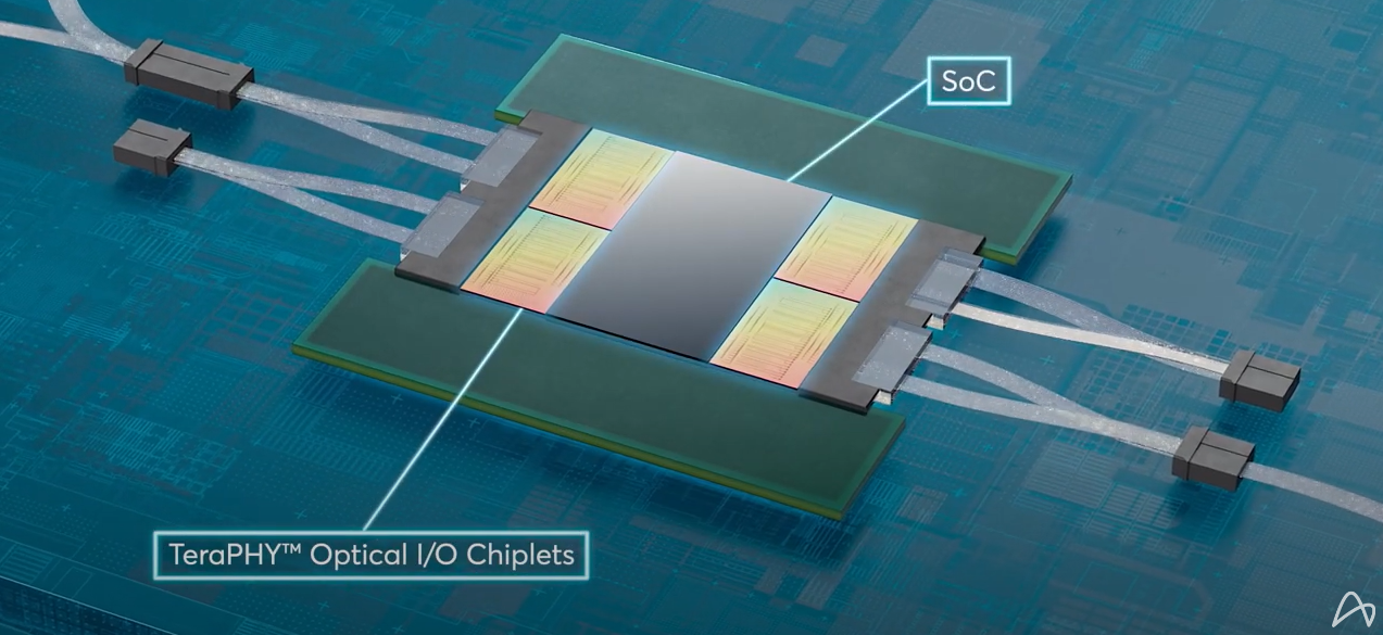
(credit: Ayar Labs)
“As soon as we … try to scale to high performance systems with 10,000 nodes, maybe even 100,000 nodes, and this is this is where the applications are driving us, (I/O) drops off by as much as two orders of magnitude,” Bergman said. “We need to improve the figure of merit by as much as five or six orders of magnitude, we need to get to multi-terabits per millimeter bandwidth densities … and we need to be at sub-pico joules per bit energies to be able to get the conductivity” needed.
Optical interconnect technology offers the promise of a bottleneck solution. Not only does the technology move data at lightning speed with minimized energy usage, it maintains its performance level regardless of the distance over which data travels, be it milometers or less as in chiplets, or kilometers as in data center infrastructures. Photonics is the key to disaggregated solutions for HPC-AI, supporting increased flexibility, efficiency, speed and reduced costs.
As Rob Ober, NVIDIA’s Chief Platform Architect, Data Center Products, has said, “The next million-X speedup will require new advanced technologies like optical I/O to support future AI and ML workloads.”
Likewise, Matt Leininger, Senior Principal HPC Strategist, Advanced Technology at Lawrence Livermore National Laboratory, said “Today, we know what technologies are necessary for the first and second generation of exascale (supercomputing) platforms in the 2022 to 2023 timeframe, but after that a crossover to optical I/O based solutions will be needed.”
The challenge for optical technology has been packaging it in a readily useable, commercialized form. Ayar Labs is a leading innovator in the photonics sector. A startup founded in 2015, Ayar Labs is funded by a number of domestic and international venture capital firms as well as strategic investors such as Applied Ventures, GlobalFoundries, Hewlett Packard Pathfinder, Intel Capital, Lockheed Martin Ventures and NVIDIA.
Ayar Labs has developed a universal optical I/O solution that uses standard silicon fabrication techniques to replace electrical-based I/O with high-speed, high-density, low-power optical chiplets and disaggregated multi-wavelength lasers. The company’s in-package optical I/O technology is the first solution to enable direct optical communications between HPC-AI system components, such as CPUs, GPUs, APUs, high bandwidth memory and pooled memory.
Ayar Labs’ electro-optical approach provides a 5x improvement in interconnect bandwidth density, as well as lower latency and reduced power requirements. Ayar Labs’ TeraPHY™ in-package optical I/O chiplet and its SuperNova™ multi-wavelength light source are building a bridge to flexible system architectures for HPC-AI.
The company’s work has garnered industry recognition. For example, last month Fast Company named Ayar Labs a recipient of a 2023 “Next Big Things in Tech” Award. The company also was named to EE Times’ Silicon 100: Startups Worth Watching in 2023, CRN’s The 10 Hottest Semiconductor Startups of 2023 (So Far), and Forbes’ America’s Best Startup Employers list.
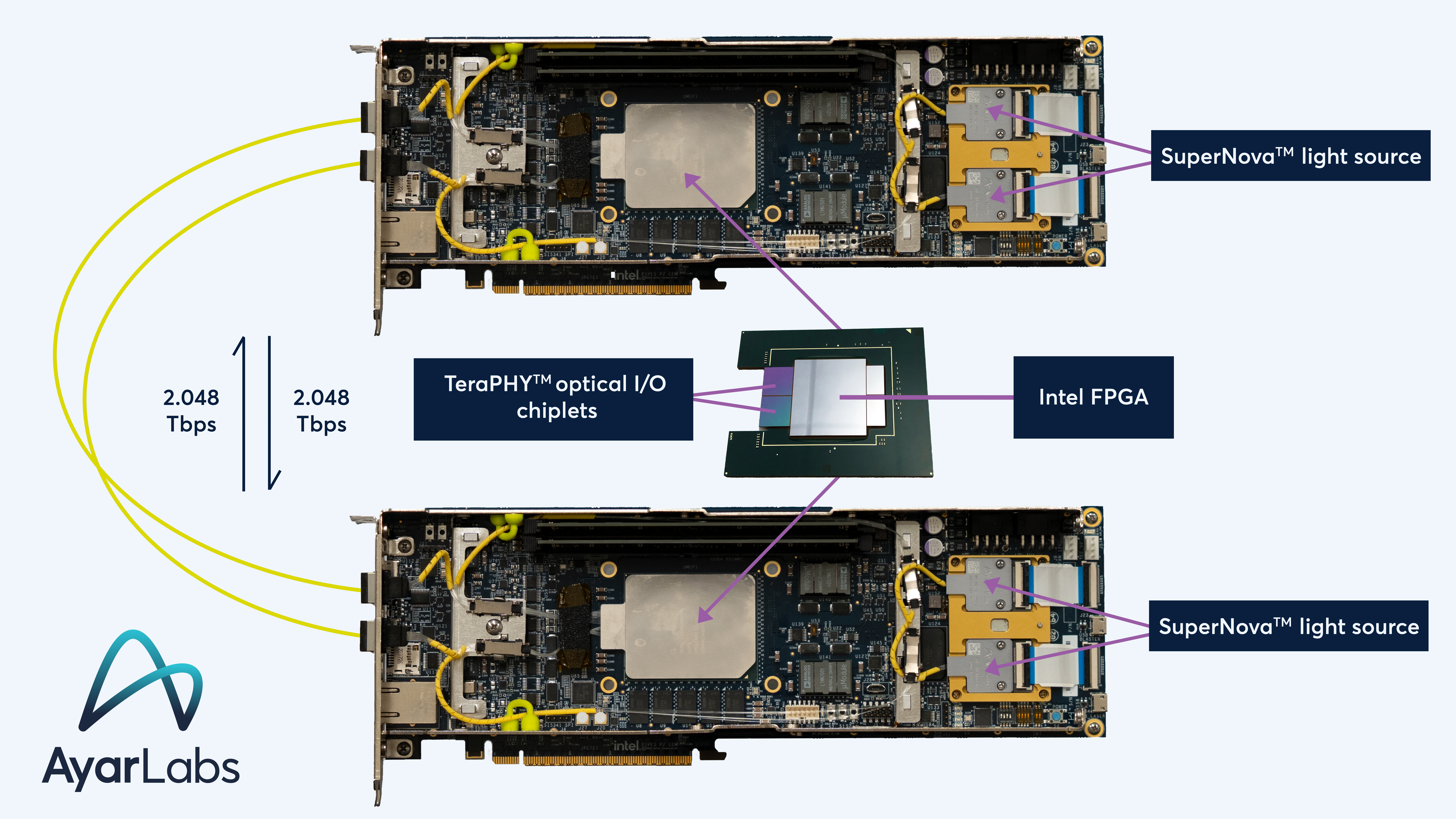
Ayar Labs showcased a 4 Tbps optically-enabled Intel FPGA design at SC23, which offers 5x current industry bandwidth at 5x lower power and 20x lower latency, all packaged in a common PCIe form factor. (credit: Ayar Labs)
At the SC23 panel, Ayar Labs’ Chief Architect and Co-Founder, Vladimir Stojanovic (he’s also a professor of EECS at the University of California, Berkeley), discussed progress made in optical I/O commercialization.
Ayar Labs’ mission, Stojanovic said, is figuring out “how can we make optics get as close to the compute chip as possible so that we essentially flatten, or enable, complete physical disaggregation of the system, to build very big, complex systems out of very small modules.”
He held up for the SC23 audience an example of Ayar Labs’ hardware.
“What I’m showing you here is a common CEM form factor PCIe card with, in this case, an Intel Agilex® FPGA SOC with two of our optical chiplets that are embedded right in this multi-chip package, together with some other SerDes chiplets from Intel,” Stojanovic said.
“This little form factor already gives you 16 links at eight terabits per second total aggregate bandwidth,” he said. “So you can imagine putting some mix of FPGAs, CPUs and GPU and memory controllers and maybe a memory card and composing the resources in a very reasonable way… Think of it as 10s of terabits per second on 30 to 60 logical links coming out of this small form factor and then you can compose, you can go build a switch fabric just by connecting a few of these cards together.
“So this is kind of what we’re trying to get at, you can build a very modular system. And remember, I’m showing you actual, real hardware. This is really running, it enables these new degrees of freedom tackling additional degrees of parallelism and mapping it back onto the system,” Stojanovic said.
With that, he encouraged his audience to visit the Ayar Labs on the SC23 conference floor for product demos in collaboration with GlobalFoundries, Ayar Labs’ manufacturing partner, along with Intel, which built the multi-chip package.

