[Sponsored Content]
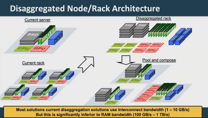
 Composable computing – a.k.a., “technology resource disaggregation” – has an allure that’s stayed strong for years. It’s an ingenious yet common-sense strategy for addressing our increasingly heterogeneous HPC-AI world where the traditional, single system approach has trouble cost-effectively supporting thefrull range of end users’ workload requirements, resulting in under-utilized, “marooned” compute resources that sap budgets. But a composable HPC infrastructure offers pools of compute, memory and storage for dynamic assembly of workload-customized, “Goldilocks” node configurations.
That said, composable HPC has its own set of challenges, one of them being connectivity between disaggregated resources along with heat generated by data movement and associated cooling costs. As is said in HPC circles: “FLOPS are cheap, moving data is expensive.”
Composable Computing – A New Path Forward
A growing consensus is emerging among HPC thought leaders that new connectivity technologies are needed to make composable computing a more practical reality for HPC-AI workloads, new ways of overcoming the bandwidth and power consumption limitations of conventional, electrical I/O. This sentiment was expressed recently by John Shalf, department head for computer science at Lawrence Berkeley National Laboratory, when he said: “Copper is always challenging to run at high speed, but also at a distance. So, we take a huge hit once we get out of the package, and an even bigger hit once we get out of the motherboard — we’re never able to recover from that.”
Shalf hosted a panel discussion on resource disaggregation in HPC at the SC21 conference and joining him were HPC experts from Japan’s RIKEN Center for Computational Science (home of “Fugaku,” the world’s most powerful supercomputer), Fujitsu (Fugaku’s system integrator), Columbia University, NVIDIA and Ayar Labs, a start-up developing new optical I/O solutions.
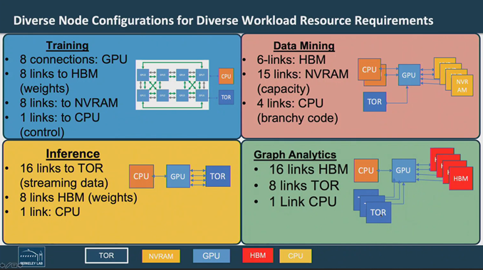
source: Berkeley Labs
In discussing the advantages of composable HPC, Shalf – also former deputy director of hardware technology for the Department of Energy’s Exascale Computing Project – focused on the difficulties of a single node architecture meeting multiple HPC-AI workload requirements.
“Our current server architecture,” he said, “what we do – especially as new accelerators come along, like GPUs, and adding solid-state storage – we pack all the possible things you could possibly need into each node, and then you replicate in order to build up a homogeneous system even though some of these jobs might not want to use the SSD, or other jobs might not want to use a GPU or whatnot.”
He cited a typical machine learning scenario in which GPUs in a training node are configured with high-bandwidth GPU-to-GPU NVLinks “so they can each train independently and then exchange weights to build up the model and to accelerate” the training process. But in an ML inference scenario, “you want to face all of your bandwidth to the top-of-rack switch and stream data in from the outside world on that trained model.” By contrast, a data mining workload may need MDRAM connectivity to find patterns within data, while graph analytics calls for high bandwidth memory and inter-node connectivity.
Backing his point, Shalf cited a study by NERSC (the National Energy Research Scientific Computing Center) finding that for each node, at least 15 percent of the workload uses more than 75 percent of the memory, justifying nodes with 128 GB of memory. Yet 75 percent of those job hours use less than 25 percent of the available memory. “That means there’s a huge amount of memory is in each node,” that is an underutilized capital and a power cost… “so having a one size fit all across all the nodes is wasteful.”
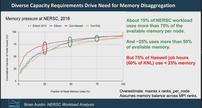
source: NERSC
Achieving HPC Scale Disaggregation with Optical I/O
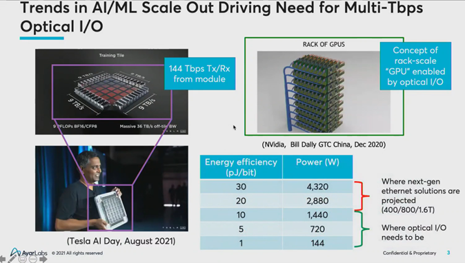
But in moving away from one-size-fits-all nodes and toward a fit-to-workload composable approach, how can composable be made to work at HPC scale? And what kind of scale are we talking about? Mark Wade, CTO at Ayar Labs, cited a presentation by Ganesh Venkataramanan, Tesla’s Senior Director of Autopilot Hardware, at the recent Tesla AI Day in which he discussed an AI compute tile with data transmit-and-receive requirements of 144 terabytes per second. Likewise, Nvidia has publicly discussed composing rack-scale GPUs so that they behave like a single, logical compute system, Wade said, enabled by optical I/O technology that can span the distance between compute nodes.

Ayar Labs CTO Mark Wade
“Solving this bandwidth distance problem, that’s really the fundamental problem,” Wade said. “We need a way to build these disaggregated systems that can span large distances and still move high bandwidths between points in those systems. And that gives us a key ingredient to being able to disaggregate compute, accelerators, memory storage – all of it.”
Optical I/O makes it possible.
“It’s creating this revolution,” Shalf said. “Whereas we used to have the high bandwidth memories sharing a package with the GPU… there’s limited area in that package. And there’s also limited reach when you’re using electronic wires to get to those packages. Instead of for the high bandwidth memory, if we can use that area to actually put down a photonic system and package … once you go from the electronic to the photonic domain, now we can go long distances without any loss and maintain that bandwidth.”
Joining Shalf and Wade on the SC21 panel was Keren Bergman, the Charles Batchelor Professor of Electrical Engineering at Columbia University, where she also directs the Lightwave Research Laboratory. In discussing her work, Bergman said she has dual priorities: high performance interconnect combined with energy efficiency.
source: Ayar Labs
The photonics R&D pursued by Bergman and her team at Columbia includes node development work with Intel, with bandwidth densities of at least a terabit per link per pin, and “we’re looking at doing multiple terabytes even per pin.” She said the key to achieving her energy efficiency objectives is utilization of a single laser that can generate up to hundreds of optical wavelengths, eliminating the need for optical amplifiers and other devices, she said.
“So, the concept is that we can have terabits to begin with – and 2 terabits in the near future and multi-terabits going forward – per pin included as part of the I/O directly to the chip,” Bergman said. “This is our vision, to directly feed potentially a large bank of high bandwidth memory, GPUs and other computing resources to really allow the deep disaggregation at the point where we have extremely high bandwidth today.”
On the power consumption front, Bergman said this technology, including laser source, thermal tuning and other elements, demonstrated at the rate of 0.5 picojoules per bit.
The New Technologies are Arriving
Bergman’s comments point to advanced-stage I/O product development occurring in the industry involving combinations of increasingly mature technologies.
“The new technologies are finally arriving,” said panel participant Satoshi Matsuoka, director of the RIKEN Center, “like stacking, photonics, signaling, etc., to greatly reduce the energy of data movement whereas FLOPS will saturate as transistor power will become constant over time irrespective of the lithography advances.”
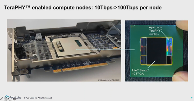
Echoing that thought was Ayar Labs’ Wade. “We’re experiencing a confluence of advanced packaging technologies combined with some of the latest advances in silicon photonics,” he said. “This has resulted in the ability to build optical I/O chiplets – single pieces of silicon that are built in a commercial, 300mm CMOS production foundry. Our chiplets are monolithic; we put all the electrical parts of the system and the optical on single chips. This then gives us a single chiplet that can intercept where the commercial production world is with advanced packaging.”
Ayar Labs’ optical I/O chiplet, called TeraPHY™, uses standard silicon fabrication techniques along with disaggregated multi-wavelength lasers to achieve high-speed, high-density chip-to-chip communication, with power consumption of between 1 and 10 picojoules. This contrasts with next-gen Ethernet solutions, which are expected to be in the 20 to 30 picojoule range, Wade said.
The result is a platform incorporating a compute ASIC (be it CPU, GPU FPGA or some kind of SOC) and optical I/O chiplets closely integrated in a 2.5-D package.
“We can build these wide parallel interfaces between the host ASIC and our chip,” Wade said. “That’s how we get electrical data in and out of our chip. And then we attach fiber to these chips. So, what you have is optical connections coming straight from the compute package.”
With TeraPHY chiplets in a disaggregated HPC infrastructure, Wade said “you can go tens of centimeters across the same board, you can go a couple of meters in the same rack, or you can go up to a couple of kilometers across a data center to a different section of racks. So, it gives you a single physical architecture that can span all these distances, and it fundamentally breaks the traditional bandwidth distance trade-off.”
For more information about disaggregated system architectures and in-package optical I/O see Ayar Labs’ most recent webinar.