HPC demands the greater throughput, lower latency, and improved power efficiency promised by in-package optical interconnects
[SPONSORED GUEST ARTICLE] Modern HPC (high performance computing) and AI (artificial intelligence) workloads are pushing the boundaries of current system architectures. Vendors continue to respond with ever-increasing performance for CPUs and GPUs, and platform designs that leverage parallel processing, packaging innovations (such as chiplet technology) and greater processor and memory density.
Unfortunately, banking on the future of HPC by deploying a large volume of processors — essentially, throwing chips at the problem — using existing interconnect solutions is a losing proposition. It creates massive I/O bottlenecks, limiting overall processor utilization as systems spend far more time waiting on data than processing it. This creates a race to the bottom: more processors are required to make up for the compute inefficiency, which further adds to bottlenecks while significantly increasing power consumption, along with CapEx and OpEx.
In short, HPC’s insatiable consumption of compute capacity and power is shining a spotlight on chip-to-chip and node-to-node data communications, which now has the largest single impact on the cost to operate HPC systems. To overcome these issues, today’s slow and hot electrical intra-node links and expensive, low-density pluggable inter-node optical connections must be replaced with something new. The need is clear for improved off-package interconnect solutions offering greater throughput, lower latency, and improved power efficiency.
Multiple recent studies on market readiness and expectations from HPC/AI users, vendors, and industry advocates have pointed to optical I/O as the logical solution to this interconnect void.
The Impact of Optical I/O
In-package optical I/O uses light to reshape the power and performance trajectories of system design. The technology solves power density and performance per watt challenges for the next generation of HPC by enabling chip-to-chip connectivity with a fraction of the power, 10x lower latency and 5x higher data rates over a reach from millimeters to kilometers versus existing electrical I/O solutions.
A 2023 study by Hyperion Research surveyed users and vendors about the future of HPC. The study found both groups aligned on the sentiment that, of seven common HPC advances, optical I/O connectivity promises to be the highest impact technology on system architectural challenges in the immediate term (one-two years) and near term (four-six years). After optical I/O, in-memory computing was expected to have the next highest impact, while physical interface standards for chiplets (e.g., UCIe) came in third. Notably, interfaces such as UCIe can enable standardized connection between the host SoC and in-package optical I/O chiplets, directly impacting adoption of optical I/O technology. These and other priorities can be seen in the chart below.
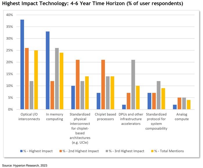
There were other interesting observations from the research: More the 75 percent of respondents agreed there is a strong need for disaggregation of system resources to enable workload-driven composable infrastructure, pointing to the need for optical I/O connectivity to support these new architectures. The largest percentage of users (about 35 percent) identified I/O bandwidth and compute-to-memory as the most critical interconnect/network bottleneck. In terms of the most critical HPC bottleneck, a plurality of about 26 percent identified memory bandwidth. Looking forward, system scale-out and network throughput are the highest priorities among respondents considering future architecture.
The CHIPS Act and Silicon Photonics
Earlier this year, the Commerce Department tasked an industry advisory committee (IAC) composed of researchers, academics, corporations, and vendors to study and provide recommendations on R&D investment for the CHIPS Act. Interestingly, the group singled out silicon photonics, of which optical I/O is a part, as the one technology most worthy of additional investment.
“If the IAC were to call out one emerging technology to receive special attention, we believe silicon photonics is a rare general-purpose technology that should merit CHIPS Act investments in R&D, prototyping, and manufacturing” — IAC R&D Gaps Report, June 6, 2023
The report went on to say that:
- Basic photonics technology can scale out across many application domains, starting first in HPC/data centers and in life sciences, and expanding to industrial, automotive, RF, computing, and quantum.
- Photonics is on the cusp of achieving significant manufacturing volumes; it is mostly unoccupied territory and the advent of CXL and UCIe chip interconnect standards paves the way for nearer-in photonics co-packaged solutions.
- The US has significant R&D capabilities, lots of startups, and investments in a photonics ecosystem and prototyping via the AIMS Photonics Mfg. USA Institute (NY), as well as commercial facilities such as GlobalFoundries (New York) and Intel (Arizona).
- Silicon photonics is one of the technologies that can address sustainability and environmental issues (energy and power reduction) across several critical applications.
- Silicon photonics, integrated with electronics, represents a fundamental leadership play if manufacturing and scaling issues can be resolved such as laser/fiber attach, electronics/photonics testing, packaging, chiplets.
Optical I/O at SC23
All of which puts a spotlight on optical I/O at Supercomputing 2023. Leading semiconductor companies including Intel and NVIDIA are pouring funds into commercializing the technology, while HPC vendors such as Hewlett Packard Enterprise and others have strategic collaborations in place to develop next-generation data center and networking architectures that would leverage optical I/O.
Ayar Labs will be showcasing its co-development (with Intel) of a seamless integration of the company’s TeraPHY™ optical I/O chiplets and SuperNova™ light sources into the same package with an Intel FPGA, delivered in a standard PCIe card form factor. This achievement brings together optical I/O design, fabrication, packaging, and overall integration, in a standard form factor, enabling usage models across multiple applications and computing platforms, including disaggregated HPC architectures.
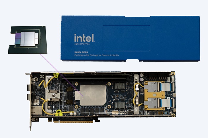
Ayar Labs/Intel integration of TeraPHY™ optical I/O chiplets and SuperNova™ light sources into the same package with an Intel FPGA, delivered in a standard PCIe card form factor.
This marks an industry milestone. While FPGAs connected to pluggable optics have existed for some time, they traditionally rely on Ethernet, with current pluggable optics typically providing 100- or 400-Gbps speeds. The integration of optics in-package accelerates performance up to 4-Tbps bi-directional, error-free, and without the Ethernet latency hit.
In a recent announcement, Venkat Yadavalli, Intel Corporation’s VP and GM, Product Excellence Group, noted, “At Intel, we pursue relentless innovation with our FPGA portfolio. With Ayar Labs’ in-package optics coupled with our FPGA fabric die, we created I/O bandwidth over 4 Tbps — far greater than what is currently possible with electrical connections. We’re looking well beyond 400G Ethernet with this capability. Optical interfaces like these have the potential to unlock huge advancements in high performance computing, AI, data centers, sensing, communications, edge, and more.”
This integration work between Ayar Labs and Intel is also noteworthy in developing heterogeneous chiplet-based architectures, combining chips in different process nodes and technologies from different vendors into a single package. Notably, this co-packaged integration development does not require any change to Intel’s FPGA, the core computing component.
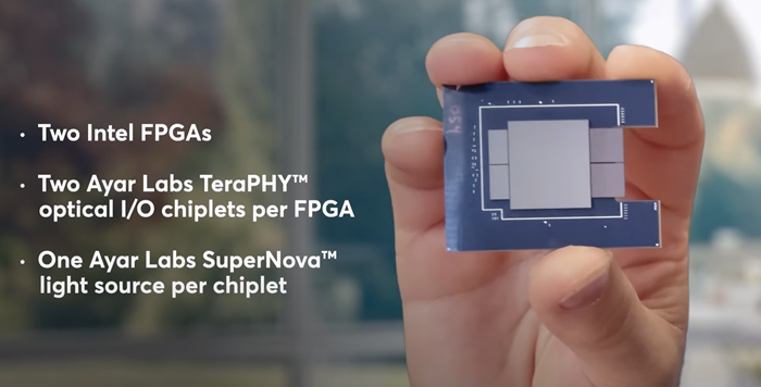
The Intel/Ayar Labs optical FPGA includes an Intel FPGA with two Ayar Labs TeraPHY optical I/O chiplets in a single package, plus one Ayar Labs SuperNova remote light source per chiplet.
Expanding Opportunities for Optical I/O
Integration of optical I/O with an FPGA is the tip of the iceberg. The vision is to enable new HPC/AI architectural advances through ubiquitous optical interconnects for every piece of compute silicon. If you are attending SC23 November 12-17, be sure to visit Ayar Labs in booth #228 for an exclusive look at the future of optical I/O. You can also hear the latest from company executives on panels discussing the Chiplet Ecosystem in High Performance Computing, AI/ML and Data Acceleration (Wednesday, November 15, 3:30-5pm) and Scalable and Adaptable Architectures for AI/HPC Advancement (Thursday, November 16, 1:30-3pm). Not attending SC23? No problem! You can also check out the optical FPGA demo in this video.