TSMC announced it has signed a preliminary agreement with the U.S. Dept. of Commerce for up to $6.6 billion under the CHIPS and Science Act. TSMC also announced plans to build a third fab at its TSMC Arizona site in Phoenix using 2nm or more advanced processes, with production beginning by the end of the decade.
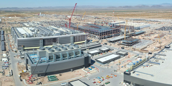
TSMC said that as the company continues construction of its first two Arizona fabs, the third fab brings TSMC’s total capital spending on the Phoenix site (pictured here) to more than $65 billion, which TSMC said is the largest foreign investments in a U.S. greenfield project.
As reported last week, TSMC said its first Arizona fab is on track to begin production leveraging 4nm technology in first half of 2025, while the second fab will produce 2nm process technology with nanosheet transistors in addition to the previously announced 3nm technology, with production beginning in 2028.
TSMC Arizona’s three fabs will create approximately 6,000 jobs. Also, according to an analysis by the Greater Phoenix Economic Council, the investment in three fabs will create more than 20,000 construction jobs and tens of thousands of indirect supplier and consumer jobs.
The company said each of the fabs will have cleanroom area approximately double the size of an industry standard logic fab.
“The CHIPS and Science Act provides TSMC the opportunity to make this unprecedented investment and to offer our foundry service of the most advanced manufacturing technologies in the United States,” said TSMC Chairman Dr. Mark Liu. “Our U.S. operations allow us to better support our U.S. customers, which include several of the world’s leading technology companies. Our U.S. operations will also expand our capability to trailblaze future advancements in semiconductor technology.”
TSMC practices green manufacturing and conducts ongoing R&D into energy efficiency, water conservation, waste management, and air pollution control. The company said TSMC Arizona’s fabs aims to achieve a 90 percent water recycling rate, and the company is designing an industrial water reclamation plant with a goal of “near zero liquid discharge”, bringing nearly every drop of water back into the facility.
 The agreement TSMC signed with the Dept. of Commerce is called a “non-binding preliminary memorandum of terms,” which — along with the proposed $6.6 billion in funding, also proposes to provide TSMC with up to $5 billion in loans. TSMC plans to apply for U.S. Treasury Department Investment Tax Credits of up to 25 percent of the qualified capital expenditure at TSMC Arizona. The company said its financial goals are to realize a 15-20 percent revenue compound annual growth rate, 53 percent and higher gross margin, and 25 percent and higher return on equity.
“Today’s announcement highlights the strong commitment from Secretary Raimondo and the entire administration to ensure the U.S. plays a central role creating a more geographically diverse and resilient semiconductor supply chain,” said AMD Chair and CEO Lisa Su. “TSMC has a long track record of providing the leading-edge manufacturing capabilities that have enabled AMD to focus on what we do best, designing high-performance chips that change the world. We are committed to our partnership with TSMC and look forward to building our most advanced chips in U.S.”
“We congratulate TSMC for its historic investment and applaud the Commerce Department for its support,” said Jensen Huang, founder and CEO of Nvidia. “TSMC has been a long-standing partner of Nvidia since we invented the GPU and accelerated computing, and our ongoing innovation in Artificial Intelligence (AI) would not have been possible without them. We are excited to continue our partnership with TSMC as it brings cutting-edge facilities to Arizona.”


Speak Your Mind